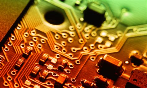
What are PCB Vias?
PCB vias are small holes drilled through a printed circuit board (PCB) that electrically connect different layers of the board. Vias allow signals and power to pass from one layer of the PCB to another. They are essential features in PCB design that enable more complex circuits and denser component placement in a smaller footprint.
There are several types of PCB vias:
| Via Type | Description |
|---|---|
| Through hole | Goes completely through the PCB from top to bottom |
| Blind | Connects an outer layer to an inner layer, but does not go through the entire board |
| Buried | Connects inner layers without being visible on the outer layers |
The size of the via depends on the PCB manufacturing capabilities and the current carrying requirements. Typical via sizes range from 0.006″ to 0.037″ in diameter.
Why Use Vias?
Vias serve several important functions in PCB design:
- Allow more complex circuitry by utilizing multiple layers
- Provide electrical connections between layers
- Conduct heat away from components
- Act as mounting holes for through-hole parts
- Enable higher density designs
Without vias, PCBs would be limited to single layer designs with components only on one side. This would severely restrict the complexity and density of the circuitry.

How to Create Vias
The via creation process involves several steps:
- Design – Vias are added to the PCB layout based on the schematic and component placement. Via size, location, and type are specified.
- Drilling – Holes are drilled or laser cut into the PCB based on the design data. The hole size is slightly smaller than the finished via size.
- Plating – A thin layer of copper is electroplated onto the entire board, including the inside of the holes, to create an electrical connection.
- Filling (optional) – The vias may be filled with a non-conductive epoxy to further strengthen the board and provide a flat surface for additional component placement.
Special care must be taken during the via creation process to ensure proper electrical conductivity and avoid defects. The via size and location must precisely match the design data. Improper plating or drilling can lead to open or short circuits.

Via Design Considerations
When adding vias to a PCB design, there are several factors to consider:
Current Carrying Capacity
The via must be large enough to carry the required current without overheating. The current carrying capacity depends on the via size, plating thickness, and the ambient temperature.
Example current carrying capacities for a 1 oz copper thickness:
| Via Diameter | Current Capacity |
|---|---|
| 0.010″ | 1.0 A |
| 0.018″ | 1.8 A |
| 0.037″ | 4.0 A |
Placement
Vias should be placed to minimize the signal path length and avoid interference with components. Vias that are too close to pads or traces can cause short circuits or manufacturing defects.
Typical via to pad spacing:
| Pad Size | Minimum Via Spacing |
|---|---|
| 0.025″ | 0.008″ |
| 0.050″ | 0.016″ |
| 0.100″ | 0.024″ |
Aspect Ratio
The aspect ratio is the ratio of the via depth to its diameter. High aspect ratios can cause issues with plating uniformity and reliability.
Typical maximum aspect ratios:
| Via Type | Aspect Ratio |
|---|---|
| Through hole | 8:1 |
| Blind/buried | 0.75:1 |
Thermal Relief
Vias that connect to large copper pours, such as ground or power planes, may need thermal relief to avoid solder wicking and tombstoning during assembly. Thermal reliefs are small traces that connect the via to the copper pour while limiting the heat transfer.
Thermal relief patterns:
| Pattern | Description |
|---|---|
| Spokes | 4 thin traces radiating from via |
| Web | Grid of thin traces surrounding via |

Via Manufacturing Defects
Despite careful design and process control, via defects can still occur during manufacturing. Common defects include:
- Misplaced or missing vias
- Vias not drilled to the correct depth
- Incompletely plated vias
- Contamination or blockage inside the via
- Fractured or cracked vias
Via defects can cause open or intermittent connections, leading to board failures in the field. Thorough inspection and testing are necessary to identify and correct any issues before the boards are assembled.
DIY Via Methods
For prototyping and small scale production, it is possible to create vias using DIY methods. These methods are not suitable for high volume or high reliability applications, but can be useful for quickly testing a design.
Hand Drilling
Vias can be manually drilled using a small drill press or rotary tool. The process is time consuming and requires a steady hand to avoid damaging the board. The hole size and placement accuracy will be limited.
Rivets
Copper rivets can be inserted into drilled holes and soldered in place to create a conductive path between layers. This method is simple but does not scale well to larger designs.
Conductive Epoxy
A conductive epoxy can be injected into the via holes to create an electrical connection. The epoxy must be cured and sanded flush with the board surface before additional processing. This method can be messy and may not provide a reliable connection.
FAQ
What is the smallest via size possible?
The minimum via size depends on the PCB manufacturing process and the design requirements. For standard PCBs, the smallest via is typically around 0.006″ in diameter. High density interconnect (HDI) PCBs can have vias as small as 0.004″.
How do I calculate the current carrying capacity of a via?
The current carrying capacity of a via can be estimated using the IPC-2221 standard formula:
I = 0.048 * dT^0.44 * A^0.725
Where:
– I = Current in amps
– dT = Temperature rise above ambient in °C
– A = Cross-sectional area of via in mils^2
For example, a 0.018″ diameter via with a 1 oz copper thickness can carry approximately 1.8A with a 10°C temperature rise.
What is via-in-pad?
Via-in-pad is a design technique where the via is placed directly on a component pad, rather than being separated by a trace. This allows for higher density placement but requires precise manufacturing control to avoid defects. Via-in-pad is commonly used for BGA and QFN packages.
Can vias be used for thermal management?
Yes, vias can be used to conduct heat away from components and into the inner layers of the board or to an external heatsink. Thermal vias are typically larger than signal vias and may be filled with a thermally conductive epoxy. They are often placed in arrays around high power components.
What is a blind via?
A blind via connects an outer layer of the PCB to an inner layer, but does not go through the entire board thickness. Blind vias are used to increase density and minimize the number of layers needed. They require additional processing steps compared to through hole vias and are more expensive to manufacture.
Conclusion
PCB vias are a critical feature in modern electronics design. They enable high density, multi-layer PCBs with complex circuitry. Proper via design and manufacturing process control are essential for reliable operation. While DIY methods can be used for prototyping, professional PCB fabrication is recommended for most applications. By understanding the key design considerations and tradeoffs, engineers can optimize their designs for performance, cost, and manufacturability.


Leave a Reply