Introduction to PCB Vias
Printed Circuit Boards (PCBs) are essential components in modern electronics. They provide a platform for mounting and connecting various electronic components, such as resistors, capacitors, and integrated circuits. One crucial aspect of PCB design is the use of vias, which are small holes drilled through the board to establish electrical connections between different layers of the PCB. In this article, we will explore the concept of PCB vias, their types, applications, and best practices for designing and manufacturing them.
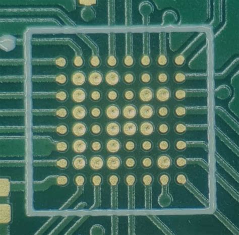
What is a PCB Via?
A PCB via is a small hole drilled through a printed circuit board to create an electrical connection between different layers of the board. Vias are typically plated with a conductive material, such as copper, to ensure reliable electrical conductivity. They allow signals and power to be routed from one layer of the PCB to another, enabling more complex and compact circuit designs.
The Importance of PCB Vias
PCB vias play a crucial role in the functionality and performance of electronic devices. They enable designers to:
- Create multi-layer PCBs: Vias allow the creation of multi-layer PCBs, which can accommodate more components and complex circuitry in a smaller footprint.
- Reduce signal interference: By using vias to route signals between layers, designers can minimize the impact of electromagnetic interference (EMI) and crosstalk.
- Improve thermal management: Vias can be used to transfer heat away from components, helping to prevent overheating and ensure reliable operation.
- Enhance signal integrity: Properly designed vias can help maintain signal integrity by reducing the length of signal paths and minimizing impedance mismatches.
Types of PCB Vias
There are several types of PCB vias, each with its own characteristics and applications. The most common types include:
Through-Hole Vias
Through-hole vias are the most basic type of via. They are drilled completely through the PCB and are typically plated with copper to create an electrical connection between layers. Through-hole vias are reliable and easy to manufacture, but they consume more board space compared to other types of vias.
Blind Vias
Blind vias are drilled from one side of the PCB and terminate at an inner layer, without passing through the entire board. They are useful for connecting an outer layer to an inner layer, allowing for more compact designs and reducing the number of layers required. Blind vias are more challenging to manufacture than through-hole vias and may increase production costs.
Buried Vias
Buried vias are located entirely within the inner layers of a PCB and do not extend to either surface of the board. They are used to connect two or more inner layers without consuming space on the outer layers. Buried vias offer the advantage of saving board space and reducing the overall size of the PCB. However, they are more complex to manufacture and can significantly increase production costs.
Micro Vias
Micro vias are small-diameter vias, typically less than 150 microns in diameter. They are used in high-density interconnect (HDI) PCBs to create fine-pitch connections between layers. Micro vias enable the design of highly compact and complex circuits, making them essential for modern electronics, such as smartphones and wearable devices.
Stacked Vias
Stacked vias are a combination of two or more vias that are aligned vertically to connect multiple layers of a PCB. They are used when a direct connection between layers is not possible due to the presence of other components or routing constraints. Stacked vias can be created using a combination of through-hole, blind, and buried vias.

PCB Via Design Considerations
Designing PCB vias requires careful consideration of various factors to ensure optimal performance, reliability, and manufacturability. Some key design considerations include:
Via Size and Aspect Ratio
The size of a via is determined by its diameter and the thickness of the PCB. The aspect ratio of a via is the ratio of its depth to its diameter. High aspect ratios can make it challenging to achieve reliable plating and may increase the risk of manufacturing defects. Designers should choose via sizes and aspect ratios that are suitable for the specific requirements of their PCB and compatible with the manufacturing capabilities of their chosen fabrication house.
Via Placement and Spacing
The placement and spacing of vias on a PCB can have a significant impact on signal integrity, EMI, and thermal management. Vias should be placed as close as possible to the components they are connecting to minimize signal path lengths and reduce the risk of signal degradation. However, vias should also be spaced far enough apart to prevent manufacturing issues, such as drill wander and copper bridging.
Via Impedance and Signal Integrity
Vias can introduce impedance discontinuities in signal paths, which can lead to signal reflections and degradation of signal quality. To minimize these effects, designers should consider the impedance of the vias and ensure that they match the impedance of the signal traces. This can be achieved through careful selection of via geometry, spacing, and the use of techniques such as ground shielding and differential pair routing.
Thermal Management
Vias can play a crucial role in thermal management by providing a path for heat to dissipate from components to the PCB substrate and ultimately to the environment. Thermal vias are often used to transfer heat away from high-power components, such as processors and power management ICs. Designers should consider the placement and density of thermal vias to ensure adequate heat dissipation and prevent component overheating.

PCB Via Manufacturing Processes
The manufacturing of PCB vias involves several processes to ensure reliable electrical connections and high-quality results. The main steps in via manufacturing include:
Drilling
Vias are created by drilling holes through the PCB substrate using specialized drilling equipment. The choice of drill bit size and material depends on the desired via diameter and the type of PCB substrate. Accurate drilling is essential to ensure proper via placement and prevent manufacturing defects.
Plating
After drilling, the vias are plated with a conductive material, typically copper, to create an electrical connection between layers. The plating process involves several steps, including cleaning, activation, and electroless copper deposition, followed by electrolytic copper plating to achieve the desired thickness.
Filling
In some cases, vias may be filled with a non-conductive material, such as epoxy or resin, to improve the structural integrity of the PCB and prevent the entrapment of contaminants. Via filling is often used in high-reliability applications, such as aerospace and military electronics.
Inspection and Testing
After the vias have been manufactured, they undergo a series of inspection and testing procedures to ensure their quality and reliability. This may include visual inspection, electrical testing, and cross-sectional analysis to verify the integrity of the plating and the absence of defects.

Best Practices for PCB Via Design and Manufacturing
To ensure the successful design and manufacturing of PCB vias, designers should adhere to the following best practices:
- Follow the design guidelines provided by the PCB fabrication house to ensure compatibility with their manufacturing capabilities and processes.
- Use industry-standard via sizes and aspect ratios to minimize the risk of manufacturing defects and ensure reliable plating.
- Place vias as close as possible to the components they are connecting to minimize signal path lengths and reduce the risk of signal degradation.
- Consider the impedance of the vias and ensure that they match the impedance of the signal traces to maintain signal integrity.
- Use thermal vias strategically to transfer heat away from high-power components and prevent overheating.
- Verify the design using simulation tools and design rule checks (DRC) to identify and resolve any potential issues before manufacturing.
- Communicate clearly with the PCB fabrication house to ensure that they understand the design requirements and can provide feedback on manufacturability and cost optimization.
Common PCB Via Defects and Challenges
Despite advancements in PCB manufacturing technologies, vias can still be subject to various defects and challenges that can impact the performance and reliability of the final product. Some common via defects include:
Drilling Defects
Drilling defects, such as drill wander, breakout, and smear, can occur during the via drilling process. These defects can lead to misaligned or incomplete vias, which can cause electrical opens or shorts and compromise the integrity of the PCB.
Plating Defects
Plating defects, such as voids, nodules, and thin or uneven plating, can occur during the via plating process. These defects can result in poor electrical connections, increased resistance, and reduced reliability of the vias.
Via Stubs
Via stubs are unused portions of a via that can act as resonant cavities, leading to signal reflections and degradation of signal quality. Via stubs are particularly problematic in high-speed digital designs and can be mitigated through the use of techniques such as back-drilling and blind vias.
Thermal Stress
Vias can be subject to thermal stress due to the mismatch in the coefficient of thermal expansion (CTE) between the PCB substrate and the plated copper. This stress can lead to via cracking and delamination, particularly in high-temperature applications or during thermal cycling.
To overcome these challenges, designers and manufacturers must work together to implement robust design practices, use advanced manufacturing technologies, and conduct thorough testing and inspection to ensure the quality and reliability of PCB vias.
Future Trends in PCB Via Technology
As electronic devices continue to become smaller, more complex, and more powerful, PCB via technology must evolve to keep pace with these advancements. Some of the future trends in PCB via technology include:
High Density Interconnect (HDI) Vias
HDI vias, such as micro vias and stacked vias, are becoming increasingly important in the design of compact and high-performance electronic devices. These vias enable the creation of fine-pitch, high-density interconnects that can accommodate the growing number of components and functions in modern electronics.
Embedded Vias
Embedded vias are a relatively new technology that involves creating vias within the PCB substrate itself, rather than drilling them after the substrate has been laminated. This approach can enable the creation of smaller, more precise vias and can help to reduce the overall thickness of the PCB.
Advanced Via Filling Materials
The development of advanced via filling materials, such as conductive pastes and nanoparticle-based materials, can help to improve the thermal and electrical performance of vias while reducing the risk of defects and failures.
3D PCB Technologies
The emergence of 3D PCB technologies, such as multi-chip modules (MCMs) and 3D stacked dies, is driving the need for more sophisticated via technologies that can enable vertical interconnects between multiple layers of components and substrates.
As these trends continue to shape the future of PCB design and manufacturing, designers and engineers must stay informed about the latest advancements in via technology and adapt their practices to ensure the creation of high-performance, reliable, and cost-effective electronic products.
Frequently Asked Questions (FAQ)
- What is the difference between a through-hole via and a blind via?
-
A through-hole via is drilled completely through the PCB, creating a connection between all layers of the board. In contrast, a blind via is drilled from one side of the PCB and terminates at an inner layer, without passing through the entire board.
-
What is the purpose of via filling?
-
Via filling is the process of filling vias with a non-conductive material, such as epoxy or resin, to improve the structural integrity of the PCB and prevent the entrapment of contaminants. Via filling is often used in high-reliability applications, such as aerospace and military electronics.
-
How can via stubs affect signal integrity?
-
Via stubs are unused portions of a via that can act as resonant cavities, leading to signal reflections and degradation of signal quality. Via stubs are particularly problematic in high-speed digital designs and can be mitigated through the use of techniques such as back-drilling and blind vias.
-
What is the role of thermal vias in PCB design?
-
Thermal vias are used to transfer heat away from high-power components, such as processors and power management ICs, to the PCB substrate and ultimately to the environment. Proper placement and density of thermal vias are essential for ensuring adequate heat dissipation and preventing component overheating.
-
What are some of the future trends in PCB via technology?
- Some of the future trends in PCB via technology include the increasing use of high-density interconnect (HDI) vias, embedded vias, advanced via filling materials, and the development of 3D PCB technologies that require sophisticated vertical interconnects between multiple layers of components and substrates.
Conclusion
PCB vias are essential components in the design and manufacturing of modern electronic devices. They enable the creation of multi-layer PCBs, reduce signal interference, improve thermal management, and enhance signal integrity. Understanding the different types of vias, their design considerations, and best practices for manufacturing is crucial for creating high-performance, reliable, and cost-effective electronic products.
As electronic devices continue to evolve, PCB via technology must also advance to keep pace with these changes. Designers and engineers must stay informed about the latest trends and advancements in via technology, such as HDI vias, embedded vias, and advanced via filling materials, to ensure that they can create products that meet the ever-increasing demands of the electronics industry.
By collaborating closely with PCB fabrication houses, adhering to best design practices, and leveraging advanced manufacturing technologies, designers can overcome the challenges associated with PCB vias and create electronic products that push the boundaries of performance, reliability, and innovation.


Leave a Reply