Introduction to Copper PCBs
Printed Circuit Boards (PCBs) are the backbone of modern electronics, providing a reliable and efficient means of connecting electronic components. Among the various types of PCBs, Thick Copper PCBs have gained significant attention due to their unique properties and applications. In this comprehensive article, we will delve into the world of thick copper PCBs, exploring their characteristics, manufacturing processes, advantages, and applications.
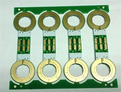
What are Copper PCBs?
Copper PCBs are printed circuit boards that utilize copper as the primary conductive material for the traces and pads. The copper layer is laminated onto a non-conductive substrate, typically made of materials such as FR-4, polyimide, or ceramic. The thickness of the copper layer can vary depending on the specific requirements of the application.
Thick Copper PCBs vs. Standard PCBs
Thick copper PCBs differ from standard PCBs in terms of the copper thickness used. While standard PCBs typically have copper thicknesses ranging from 0.5 oz to 2 oz per square foot, thick copper PCBs can have copper thicknesses of 3 oz or more per square foot. This increased copper thickness provides several advantages, which will be discussed in detail later in this article.
Manufacturing Process of Thick Copper PCBs
Substrate Selection
The first step in manufacturing thick copper PCBs is selecting an appropriate substrate material. The substrate acts as the base onto which the copper layer is laminated. Common substrate materials include:
- FR-4: A composite material made of woven fiberglass and epoxy resin, known for its excellent mechanical and electrical properties.
- Polyimide: A high-performance polymer that offers superior thermal stability and flexibility compared to FR-4.
- Ceramic: A substrate material known for its excellent thermal conductivity and dimensional stability, often used in high-temperature applications.
Copper Foil Lamination
Once the substrate is chosen, a thick copper foil is laminated onto the substrate using heat and pressure. The copper foil thickness can range from 3 oz to 20 oz or more per square foot, depending on the specific requirements of the application. The lamination process ensures a strong bond between the copper foil and the substrate, preventing delamination and ensuring the reliability of the PCB.
Patterning and Etching
After the copper foil is laminated, the desired circuit pattern is transferred onto the copper layer using photolithography. A photoresist material is applied to the copper surface and exposed to light through a photomask containing the circuit pattern. The exposed areas of the photoresist are then developed, leaving the desired pattern on the copper surface.
Next, the unwanted copper is removed through an etching process, typically using a chemical etchant such as ferric chloride or ammonium persulfate. The etching process selectively removes the copper not protected by the photoresist, leaving behind the desired Circuit Traces and pads.
Drilling and Plating
Once the circuit pattern is etched, holes are drilled through the PCB to accommodate through-hole components or to create vias for inter-layer connections. The holes are then plated with copper to ensure electrical conductivity and to protect the exposed substrate material.
Solder Mask and Silkscreen
A solder mask, typically made of a green or black polymer, is applied to the PCB surface to protect the copper traces from oxidation and to prevent Solder Bridges during the assembly process. The solder mask also provides insulation between adjacent traces.
Finally, a silkscreen layer is added to the PCB, which includes text, symbols, and component designators to aid in the assembly and troubleshooting process.

Advantages of Thick Copper PCBs
Higher Current Carrying Capacity
One of the primary advantages of thick copper PCBs is their higher current carrying capacity compared to standard PCBs. The increased copper thickness allows for larger trace widths, which can handle higher currents without overheating or suffering from voltage drops. This makes thick copper PCBs ideal for power electronics applications, where high currents are common.
Improved Thermal Management
Thick copper PCBs also offer improved thermal management capabilities. The increased copper thickness provides a larger cross-sectional area for heat dissipation, allowing the PCB to effectively transfer heat away from components. This is particularly important in high-power applications, where efficient heat dissipation is critical for ensuring the reliability and longevity of the electronic system.
Enhanced Mechanical Strength
The increased copper thickness also contributes to the enhanced mechanical strength of thick copper PCBs. The thicker copper layer provides additional rigidity and durability to the PCB, making it more resistant to mechanical stresses and vibrations. This is particularly important in applications where the PCB is subjected to harsh environmental conditions or mechanical shocks.
Lower Electrical Resistance
Thick copper PCBs exhibit lower electrical resistance compared to standard PCBs due to the increased cross-sectional area of the copper traces. Lower electrical resistance translates to reduced power losses and improved signal integrity, as the signals can travel through the traces with minimal attenuation and distortion.
Improved EMI/RFI Shielding
The increased copper thickness in thick copper PCBs also provides improved shielding against electromagnetic interference (EMI) and radio frequency interference (RFI). The thicker copper layer acts as a barrier, reducing the penetration of unwanted electromagnetic signals into the PCB and minimizing the emission of such signals from the PCB. This is particularly important in sensitive electronic systems, where EMI/RFI can cause signal degradation and malfunction.

Applications of Thick Copper PCBs
Thick copper PCBs find applications in various industries and sectors where high current handling, efficient thermal management, and mechanical strength are critical. Some of the common applications include:
Power Electronics
Thick copper PCBs are extensively used in power electronics applications, such as power supplies, motor drives, and inverters. The high current carrying capacity and improved thermal management capabilities of thick copper PCBs make them suitable for handling the large currents and heat dissipation requirements associated with power electronics.
Automotive Electronics
The automotive industry relies on thick copper PCBs for various electronic systems, such as engine control units (ECUs), power distribution modules, and battery management systems. The enhanced mechanical strength and thermal management properties of thick copper PCBs make them well-suited for the harsh operating conditions encountered in automotive environments.
Industrial Automation and Control
Thick copper PCBs are used in industrial automation and control systems, where reliability and robustness are paramount. The improved current carrying capacity and thermal management capabilities of thick copper PCBs ensure the stable and efficient operation of industrial control systems, even in demanding conditions.
Telecommunications
In the telecommunications industry, thick copper PCBs are used in high-frequency applications, such as RF power amplifiers and base station equipment. The lower electrical resistance and improved EMI/RFI shielding properties of thick copper PCBs make them suitable for handling high-frequency signals and minimizing signal distortion.
Aerospace and Defense
Thick copper PCBs find applications in aerospace and defense systems, where high reliability and performance are essential. The enhanced mechanical strength and thermal management capabilities of thick copper PCBs make them suitable for use in avionics, radar systems, and satellite communications equipment.

Thick Copper PCB Design Considerations
When designing thick copper PCBs, several key considerations need to be taken into account to ensure optimal performance and reliability. These include:
Trace Width and Spacing
The increased copper thickness in thick copper PCBs allows for wider traces and larger spacing between traces compared to standard PCBs. However, it is important to adhere to the manufacturer’s design guidelines and industry standards to ensure proper trace width and spacing for the desired copper thickness. This helps in avoiding manufacturing issues and ensuring reliable performance.
Thermal Management
While thick copper PCBs offer improved thermal management capabilities, it is still important to consider the thermal design aspects of the PCB. Proper component placement, the use of thermal vias, and the incorporation of heatsinks or other cooling mechanisms should be considered to ensure effective heat dissipation and prevent thermal issues.
Mechanical Considerations
The increased copper thickness and rigidity of thick copper PCBs can impact the mechanical design of the PCB. Factors such as board thickness, component placement, and mounting methods should be carefully considered to ensure the mechanical integrity of the PCB and to avoid any potential issues during the assembly process.
Signal Integrity
While thick copper PCBs offer lower electrical resistance and improved signal integrity, it is still important to consider signal integrity aspects when designing the PCB. Proper impedance matching, minimizing crosstalk, and ensuring appropriate signal termination should be taken into account to maintain signal integrity and avoid any signal degradation or distortion.
Manufacturing Capabilities
When designing thick copper PCBs, it is essential to consider the manufacturing capabilities of the PCB fabricator. Not all PCB manufacturers have the expertise and equipment to handle thick copper PCBs, so it is important to choose a reputable manufacturer with experience in producing thick copper PCBs. Additionally, the design should adhere to the manufacturer’s capabilities and guidelines to ensure manufacturability and avoid any potential issues during production.
Frequently Asked Questions (FAQ)
-
What is the minimum copper thickness for a PCB to be considered a thick copper PCB?
A PCB is typically considered a thick copper PCB when the copper thickness is 3 oz or more per square foot. However, the exact definition may vary depending on the manufacturer and the specific application requirements. -
Can thick copper PCBs be used for high-frequency applications?
Yes, thick copper PCBs can be used for high-frequency applications. The lower electrical resistance and improved EMI/RFI shielding properties of thick copper PCBs make them suitable for handling high-frequency signals with minimal distortion and interference. -
Are thick copper PCBs more expensive than standard PCBs?
Yes, thick copper PCBs are generally more expensive than standard PCBs due to the increased copper thickness and the specialized manufacturing processes required. However, the added cost is often justified by the improved performance, reliability, and thermal management capabilities offered by thick copper PCBs. -
Can thick copper PCBs be used in flexible circuits?
Yes, thick copper PCBs can be used in flexible circuits. Flexible substrates such as polyimide can be used in combination with thick copper layers to create Flexible PCBs with high current carrying capacity and improved thermal management properties. -
How do I select the appropriate copper thickness for my application?
The selection of copper thickness depends on various factors such as the current carrying requirements, thermal management needs, mechanical constraints, and signal integrity considerations. It is recommended to consult with a PCB design expert or the PCB manufacturer to determine the optimal copper thickness for your specific application.
Conclusion
Thick copper PCBs offer numerous advantages over standard PCBs, including higher current carrying capacity, improved thermal management, enhanced mechanical strength, lower electrical resistance, and improved EMI/RFI shielding. These properties make thick copper PCBs suitable for a wide range of applications, including power electronics, automotive electronics, industrial automation, telecommunications, and aerospace and defense.
When designing thick copper PCBs, it is important to consider various factors such as trace width and spacing, thermal management, mechanical considerations, signal integrity, and manufacturing capabilities. By carefully addressing these design considerations and working with experienced PCB manufacturers, engineers can harness the full potential of thick copper PCBs and create reliable, high-performance electronic systems.
As technology continues to advance and the demand for high-power, thermally efficient, and mechanically robust electronic systems grows, thick copper PCBs will likely play an increasingly important role in shaping the future of electronics. By understanding the characteristics, manufacturing processes, advantages, and applications of thick copper PCBs, engineers and designers can make informed decisions and leverage this technology to push the boundaries of electronic innovation.


Leave a Reply