What is SMT Assembly?
Surface-mount technology (SMT) is a method for producing electronic circuits in which the components are mounted directly onto the surface of printed circuit boards (PCBs). An electronic device so made is called a surface-mount device (SMD). In industry, this approach has largely replaced the through-hole technology construction method of fitting components, in large part because SMT allows for increased manufacturing automation which reduces cost and improves quality. It also allows for more components to fit on a given area of substrate.
SMT assembly is the process of mounting components onto a PCB using surface mount technology. The main steps in the SMT assembly process are:
- Solder Paste Printing
- Component Placement
- Reflow Soldering
- Inspection
Solder Paste Printing
The first step in SMT assembly is to print solder paste onto the PCB pads using a solder paste stencil. The stencil is a thin sheet of stainless steel with holes cut out where the solder paste needs to be deposited. The PCB is placed in a stencil printer and solder paste is spread across the stencil using a squeegee blade, forcing paste through the holes onto the pads.
Key parameters that need to be controlled in this step are:
- Print speed
- Print pressure
- Stencil thickness
- Aperature size/shape
- Paste viscosity
- Paste roll
An inspection is typically performed after printing to ensure proper paste deposit. This can be done using 2D or 3D optical inspection systems.
Component Placement
After solder paste printing, the PCB moves to a pick-and-place machine which mounts the SMT components onto their pads. The components, which come packaged in tape-and-reel, stick, or tray format, are picked up from the packaging by a vacuum nozzle and placed precisely on their pads.
Modern pick-and-place machines are extremely fast and accurate, capable of mounting tens of thousands of components per hour with placement accuracies of 50 microns or better. Key parameters include:
- Placement force
- Placement accuracy
- Nozzle type (vacuum, gripper)
- Component size/pitch
- Board support
There is usually a post-placement inspection to verify all components are present and positioned correctly before reflow.
Reflow Soldering
After component placement, the PCBs are conveyed through a reflow oven, which melts the solder paste and permanently attaches the components to the board. The reflow profile is carefully controlled, taking the PCB and components through a controlled preheat, reflow, and cooling phases.
The reflow profile needs to be optimized based on:
- Solder paste (alloy, flux)
- Component types
- PCB Thickness, layer count
- Reflow oven type (IR, convection, vapor phase)
The peak reflow temperature is typically 20-40°C above the melting point of the solder alloy for a period of 30-90 seconds. Common reflow profiles for lead-free solder pastes are shown below:
| Profile | Preheat Rate (°C/s) | Soak Temp (°C) | Soak Time (s) | Peak Temp (°C) | Time Above Liquidus (s) | Cooling Rate (°C/s) |
|---|---|---|---|---|---|---|
| Linear | 0.5-2 | 150-180 | 60-120 | 235-245 | 30-90 | 2-6 |
| Soak | 0.5-2 | 150-180 | 60-120 | 235-245 | 30-90 | 2-6 |
| Ramp-Soak-Spike | 0.5-2 | 150-180 | 60-120 | 260-270 | 20-40 | 2-6 |
Table 1. Common lead-free reflow profiles.
The reflow step transforms the solder paste into shiny solder fillets that form a strong mechanical and electrical connection. Voids, solder balls, bridging, or poor wetting can occur if the reflow profile is not properly optimized.
Inspection
Post-reflow inspection is critical to identify any solder joint defects or component issues. Automated optical inspection (AOI) systems are commonly used to check for problems like:
- Missing/misaligned components
- Lifted leads
- Solder bridges
- Insufficient/excess solder
- Damaged components
Electrical testing may also be performed at this stage to verify proper connectivity and functionality of the assembly. X-ray inspection allows detection of subsurface defects like voids that may not be visible optically.
First pass yield is a key metric tracked in SMT assembly. This refers to the number of defect-free boards coming out of the line without needing any rework or repair. World-class SMT assembly processes can achieve first pass yields of 99% or greater.
Benefits of SMT Assembly
SMT assembly provides many advantages compared to through-hole assembly:
- Increased circuit density – Smaller SMT components allow more functionality in a smaller space
- Faster assembly – High-speed equipment enables much higher throughput vs manual insertion
- Lower cost – Automation reduces labor costs, and SMT components are generally cheaper
- Improved quality – The SMT process is more repeatable and consistent than through-hole
- Double-sided assembly – Components can be mounted on both sides of the PCB
These benefits have made SMT the standard assembly technology for the vast majority of electronic products being manufactured today, from smartphones to servers to LED light bulbs. Through-hole assembly is now typically only used for components that are too large for SMT (e.g. connectors, large power transistors) or products that require extreme reliability (aerospace, medical devices).

SMT Component Types
A wide variety of component package types are available for SMT assembly, offering varying sizes, lead pitches and configurations:
- Passive chips – Resistors and capacitors, 0201 to 2512 and larger
- SOT – Small outline transistors, SOT-23 to SOT-663
- QFP – Quad flat pack ICs, 0.4-0.8mm pitch
- QFN – Quad flat no-lead ICs, 0.4-0.65mm pitch
- BGA – Ball grid array, 0.3-1.27mm pitch
- LGA – Land grid array
- CSP – Chip scale package
- Flip chip – Direct die attach
- POP – Package on package
Table 2. Common SMT package types.
| Package | Pitch (mm) | Size L x W (mm) | Height (mm) |
|---|---|---|---|
| 0201 | N/A | 0.6 x 0.3 | 0.23 |
| 0402 | N/A | 1.0 x 0.5 | 0.35 |
| 0603 | N/A | 1.6 x 0.8 | 0.45 |
| 0805 | N/A | 2.0 x 1.25 | 0.50 |
| 1206 | N/A | 3.2 x 1.6 | 0.55 |
| SOT-23 | 0.95 | 3.0 x 1.4 | 1.1 |
| SOT-223 | 2.3 | 6.5 x 3.5 | 1.6 |
| QFP-44 | 0.8 | 10 x 10 | 1.6 |
| QFN-32 | 0.5 | 5 x 5 | 0.9 |
| BGA-121 | 1.0 | 11 x 11 | 1.7 |
Table 3. Dimensions of common SMT packages.
New component types continue to be developed to enable further miniaturization and performance improvements. The latest smartphones utilize cutting-edge packaging technologies like package-on-package (PoP), wafer-level CSP, and flip chip interconnect.

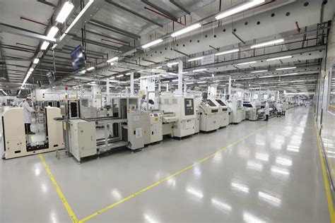
SMT Assembly Equipment
A typical SMT assembly line consists of the following equipment:
- Stencil Printer – Applies solder paste to PCB pads
- Pick-and-Place – Places components on PCB
- Reflow Oven – Melts solder paste to attach components
- AOI – Automated optical inspection for solder joint defects
- X-ray – Inspection for hidden solder joint defects
- ICT – In-circuit test for electrical defects
- Functional Test – Verifies proper operation of assembled board
In high volume production, multiple printers and pick-and-place machines may be used in parallel to increase throughput. Additional equipment that may be found in an SMT assembly line includes:
- Glue Dispenser – Applies adhesive dots to hold components
- Odd-Form Placement – For placing large/odd-shaped components
- Selective Solder – For dip soldering of through-hole components
- Conformal Coating – Applies a protective coating over the assembly
- Depaneling – Singulate individual PCBs from a panel
The total capital investment for a complete SMT assembly line can range from under $100k for a basic prototype line to tens of millions of dollars for a high-volume production line with the latest equipment. Operating costs include labor, material, electricity, consumables, and maintenance.

Design for SMT Assembly
Designing a PCB for effective SMT assembly requires consideration of several factors:
- Component Selection – Choose packages that are compatible with your assembly process
- Footprint Design – Follow manufacturer and IPC guidelines for land pattern dimensions
- Placement – Provide adequate spacing between components for pick-and-place
- Panelization – Sub-panel PCBs to fit in assembly line
- Paste Stencil – Optimize aperture size and shape for good paste release
- Reflow Profile – Select paste and components that have compatible profiles
- Testability – Include test points and other DFT features to facilitate testing
Following best practices in DfMA (Design for Manufacture and Assembly) can improve first pass yield, reduce assembly cycle time, and minimize cost. Involving your assembly partner early in the design process allows them to provide valuable feedback and catch potential issues before the design is released.
Choosing an SMT Assembly Partner
Key factors to consider when selecting an SMT assembly partner include:
- Technical Capabilities – Equipment, expertise, quality certifications
- Capacity – Ability to meet your volume and lead time requirements
- Location – Proximity to your development team and end markets
- Culture – Communication style, flexibility, customer service
- Cost – Competitive pricing for your target volumes
It’s important to conduct a thorough audit of potential assembly partners, reviewing their facility, processes, and business practices. Visiting in person is ideal to get a firsthand look at their operation. Building a close relationship with your assembly partner enables a collaborative, problem-solving approach when issues arise.
Leading SMT assembly providers offer additional value-added services like:
- Supply Chain Management – Component sourcing, inventory management, kitting
- Design Support – DFM analysis, layout reviews, test development
- Box Build – Final product assembly, packaging, logistics
- Sustaining Engineering – ECOs, failure analysis, product enhancements
The Future of SMT Assembly
SMT assembly technology continues to evolve to support the needs of advanced electronic products. Some key trends shaping the future of SMT assembly include:
- Miniaturization – Smaller chip-scale packages and fine-pitch BGAs becoming more common
- Flexibility – Faster product cycles requiring quicker changeover between builds
- Automation – Use of robots and conveyor systems to boost productivity
- Sensors – In-line monitoring of paste volume, component placement, reflow profile
- Traceability – Component-level tracking and data logging for process improvements
- Environmental – Shift to lead-free solders and Halogen-Free PCBs
To remain competitive, SMT assembly providers will need to continually invest in new equipment, processes, and skills. Those that can combine technical capabilities with supply chain expertise, design support services, and robust quality systems will be well-positioned to meet the challenges of tomorrow’s electronic assemblies.
Frequently Asked Questions
What is the smallest component that can be placed by SMT?
0201 (0.6 x 0.3mm) is the current standard for the smallest readily available and placeable component. Some cutting-edge packaging technologies like 01005 and 008004 are starting to be used but are still very niche.
What is a typical SMT assembly lead time?
Lead times vary based on complexity and volume but for a standard PCB Assembly a typical lead time is 2-3 weeks from receipt of order, assuming parts are available. Expedite services are usually available at a premium cost.
What kind of tolerances can SMT achieve?
A modern pick-and-place machine can place components with an accuracy of ±50 microns (0.05mm) or better. Solder joint dimensions are typically controlled to ±100 microns.
How much does SMT assembly cost?
SMT assembly pricing depends on many factors including the size of the PCB, number of components, volume, testing requirements, and turn time. As a rough guide, a simple single-sided assembly might cost $5-20 at mid-volume (1000s), while a complex double-sided assembly with BGAs and testing could be $50-200.
What certifications should I look for in an SMT assembly partner?
The most common quality certification for PCB assembly is ISO 9001. For automotive applications, look for IATF 16949. AS9100 covers aerospace requirements. For medical devices, ISO 13485 is the standard. IPC also has several certifications like IPC-A-610 for acceptability.


Leave a Reply