PCB Substrate Materials
The substrate is the foundation of a PCB, providing mechanical support and electrical insulation for the components and traces. The choice of substrate material depends on factors such as the intended application, operating environment, and cost. Common PCB substrate materials include:
FR-4
FR-4 is the most widely used PCB substrate material. It is a composite material made of woven fiberglass cloth impregnated with an epoxy resin. FR-4 offers good mechanical strength, electrical insulation, and thermal stability, making it suitable for a wide range of applications.
High-Frequency Laminates
For applications involving high-frequency signals, such as RF and microwave circuits, specialized substrate materials are used. These materials, such as Rogers RO4000 series and Isola IS680, have lower dielectric constants and dissipation factors, which help minimize signal loss and distortion at high frequencies.
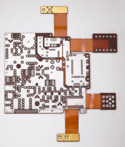
Flexible Substrates
Flexible PCBs use substrate materials that can bend and flex without damaging the circuits. Common flexible substrate materials include polyimide (Kapton) and polyester (PET). These materials are thinner and more lightweight than rigid substrates, making them ideal for applications requiring flexibility or space constraints.
Copper Foil
Copper foil is the conductive layer that forms the traces, pads, and planes on a PCB. It is typically laminated onto the substrate material using heat and pressure. The thickness of the copper foil is measured in ounces per square foot (oz/ft²), with common thicknesses being 0.5 oz/ft², 1 oz/ft², and 2 oz/ft².
Electrodeposited (ED) Copper
ED copper is the most common type of copper foil used in PCBs. It is manufactured by electroplating copper onto a drum or carrier foil, resulting in a smooth, shiny surface. ED copper offers good solderability and adhesion to the substrate.
Rolled Annealed (RA) Copper
RA copper is produced by mechanically rolling copper foil to the desired thickness. It has a matte surface finish and higher elongation compared to ED copper, making it more suitable for flexible PCBs and applications requiring better mechanical properties.
Solder Mask
Solder mask is a protective layer applied over the copper traces on a PCB. It serves several purposes, including:
- Preventing accidental short circuits by insulating the copper traces
- Protecting the copper from oxidation and environmental damage
- Providing a surface for applying component designators and labels
- Improving the aesthetics of the PCB
Solder mask is typically applied using a screen printing or photoimaging process and is available in various colors, with green being the most common.

Silkscreen
Silkscreen, also known as legend or nomenclature, is a layer of text and symbols printed onto the solder mask. It provides important information such as component designators, polarity markers, and logos. Silkscreen is typically printed using a screen printing process and is available in various colors, with white being the most common.

Surface Finishes
Surface finishes are applied to the exposed copper pads and traces on a PCB to improve solderability, protect against oxidation, and enhance the electrical and mechanical properties of the connections. Common surface finishes include:
Hot Air Solder Leveling (HASL)
HASL is a popular surface finish that involves dipping the PCB in molten solder and then using hot air to level the solder on the pads and traces. HASL provides good solderability and is relatively inexpensive, but it can result in an uneven surface and is not suitable for fine-pitch components.
Electroless Nickel Immersion Gold (ENIG)
ENIG is a two-layer surface finish consisting of a thin layer of gold over a layer of nickel. The nickel layer provides a barrier against copper diffusion, while the gold layer offers excellent solderability and oxidation resistance. ENIG is suitable for fine-pitch components and has a long shelf life.
Immersion Silver (ImAg)
ImAg is a single-layer surface finish that deposits a thin layer of silver onto the copper pads and traces. It offers good solderability and is less expensive than ENIG, but it has a shorter shelf life and can tarnish over time.
Organic Solderability Preservative (OSP)
OSP is a thin, transparent organic coating applied to the copper pads and traces. It provides temporary protection against oxidation and improves solderability. OSP is relatively inexpensive and has a low environmental impact, but it has a limited shelf life and requires careful handling.
Via Types
Vias are conductive pathways that connect different layers of a multi-layer PCB. They allow signals and power to be routed between layers, enabling more complex circuit designs. Common via types include:
Through-hole Vias
Through-hole vias are drilled completely through the PCB and are typically plated with copper to provide electrical connectivity between layers. They are the most common type of via and are suitable for most applications.
Blind Vias
Blind vias are drilled from one surface of the PCB to an inner layer, but do not pass through the entire board. They are used to connect outer layers to inner layers and can help reduce the size of the PCB.
Buried Vias
Buried vias are located entirely within the inner layers of a PCB and do not connect to either surface. They are used to connect inner layers to each other and can help improve signal integrity and reduce electromagnetic interference (EMI).
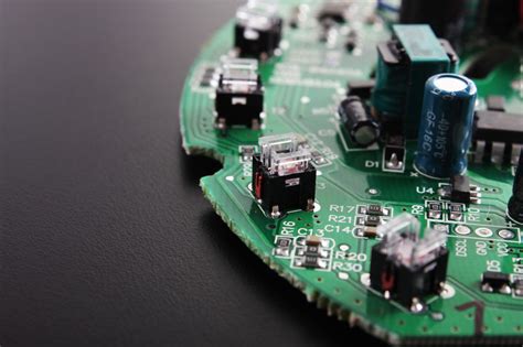
Component Types
PCBs are designed to accommodate various types of electronic components, each with their own package styles and mounting requirements. Common component types include:
Through-hole Components
Through-hole components have leads that are inserted through drilled holes in the PCB and soldered to pads on the opposite side. They are typically larger and more robust than surface-mount components and are suitable for applications requiring high mechanical strength or power handling.
Surface-mount Components
Surface-mount components are mounted directly onto pads on the surface of the PCB. They are smaller and more compact than through-hole components, allowing for higher component density and smaller PCB Sizes. Surface-mount components are widely used in modern electronics due to their space-saving and cost-effective nature.
Ball Grid Array (BGA) Components
BGA Components have an array of solder balls on their underside that connect directly to pads on the PCB surface. They offer high pin density and improved thermal and electrical performance compared to other package types. BGA components are commonly used for high-performance Integrated Circuits such as processors and FPGAs.
PCB Assembly Process
The PCB assembly process involves several steps to populate the board with components and create a functional circuit. The main steps in the assembly process are:
- Solder Paste Application: Solder paste, a mixture of tiny solder particles and flux, is applied to the pads on the PCB using a stencil or screen printing process.
- Component Placement: Components are placed onto the solder paste-covered pads using automated pick-and-place machines or manual assembly methods.
- Reflow Soldering: The PCB is heated in a reflow oven, causing the solder paste to melt and form a strong electrical and mechanical bond between the components and the pads.
- Inspection and Testing: The assembled PCB undergoes visual inspection and electrical testing to ensure proper functionality and quality.
- Conformal Coating (Optional): A protective coating may be applied to the PCB to provide additional insulation, moisture resistance, and protection against environmental factors.
FAQ
- What is the difference between a single-layer and a multi-layer PCB?
A Single-Layer PCB has conductive traces on only one side of the substrate, while a multi-layer PCB has conductive traces on multiple layers, separated by insulating layers. Multi-layer PCBs allow for more complex circuits and higher component density.
- Can PCBs be recycled?
Yes, PCBs can be recycled to recover valuable materials such as copper, gold, and other metals. However, the recycling process is complex and requires specialized facilities to ensure proper handling and disposal of hazardous substances.
- What is the purpose of vias in a PCB?
Vias are conductive pathways that connect different layers of a multi-layer PCB. They allow signals and power to be routed between layers, enabling more complex circuit designs and reducing the overall size of the PCB.
- How do I choose the appropriate surface finish for my PCB?
The choice of surface finish depends on factors such as the intended application, component types, soldering process, and environmental requirements. Consider the solderability, shelf life, and cost of each surface finish option and consult with your PCB manufacturer for recommendations.
- What is the difference between through-hole and surface-mount components?
Through-hole components have leads that are inserted through drilled holes in the PCB and soldered to pads on the opposite side. Surface-mount components are mounted directly onto pads on the surface of the PCB. Surface-mount components are generally smaller and more compact than through-hole components, allowing for higher component density and smaller PCB sizes.
Conclusion
PCBs are complex assemblies that rely on a variety of materials and components to function properly. Understanding the basic components of a PCB, including the substrate, copper foil, solder mask, silkscreen, surface finishes, via types, and component types, is essential for designing, manufacturing, and assembling reliable and high-quality electronic devices.
By carefully selecting the appropriate materials and components for a given application and following best practices for PCB design and assembly, engineers and manufacturers can create PCBs that meet the demanding requirements of modern electronics. As technology continues to advance, new materials and techniques will emerge, further expanding the capabilities and applications of PCBs in the ever-evolving world of electronics.


Leave a Reply