Introduction to Heavy copper PCB
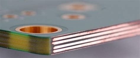
Heavy Copper PCBs, also known as thick copper PCBs, are printed circuit boards that feature copper traces thicker than the standard 1 oz (35 μm) thickness. These PCBs are designed to handle high current applications, improve thermal management, and enhance the overall reliability of electronic devices. The increased copper thickness allows for better electrical conductivity, reduced resistance, and improved heat dissipation.
Applications of Heavy Copper PCB
Heavy copper PCBs find applications in various industries and sectors, including:
- Power electronics
- Automotive electronics
- Industrial control systems
- Telecommunications equipment
- Medical devices
- Aerospace and defense systems
- Renewable energy systems
The use of heavy copper PCBs in these applications ensures better performance, reliability, and longevity of the electronic components and devices.
Advantages of Heavy Copper PCB
1. Improved Current Carrying Capacity
One of the primary advantages of heavy copper PCBs is their ability to handle higher currents compared to standard PCBs. The increased copper thickness allows for better current carrying capacity, reducing the risk of overheating and thermal damage to the components. This is particularly important in power electronics applications where high currents are common.
2. Enhanced Thermal Management
Heavy copper PCBs offer improved thermal management capabilities due to the increased copper content. Copper is an excellent thermal conductor, and the thicker traces help dissipate heat more efficiently from the components to the surrounding environment. This reduces the risk of thermal stress and improves the overall reliability of the electronic device.
3. Reduced Resistance and Voltage Drop
The thicker copper traces in heavy copper PCBs result in reduced resistance and voltage drop across the board. This is crucial in applications where maintaining a stable voltage supply is essential for proper functioning of the electronic components. Lower resistance also contributes to improved power efficiency and reduced power loss.
4. Better Mechanical Strength
Heavy copper PCBs offer better mechanical strength compared to standard PCBs. The increased copper thickness provides additional rigidity to the board, making it more resistant to physical stress and vibrations. This is particularly important in applications where the electronic device is subjected to harsh environmental conditions or mechanical shocks.
5. Improved Reliability and Longevity
The combination of improved current carrying capacity, enhanced thermal management, reduced resistance, and better mechanical strength contributes to the overall reliability and longevity of heavy copper PCBs. These boards are less prone to failures caused by thermal stress, electrical overload, or mechanical damage, resulting in a longer operational life for the electronic device.

Heavy Copper PCB Manufacturing Process
The manufacturing process for heavy copper PCBs is similar to that of standard PCBs, with a few additional steps to accommodate the increased copper thickness. The process typically involves the following stages:
-
Design and Layout: The PCB design is created using specialized software, taking into account the specific requirements of the heavy copper application.
-
Substrate Preparation: The PCB Substrate, typically FR-4, is cleaned and prepared for the subsequent manufacturing steps.
-
Copper Deposition: The thick copper layer is deposited onto the substrate using electroplating or other suitable methods. The copper thickness can range from 2 oz to 14 oz or more, depending on the application requirements.
-
Patterning and Etching: The copper layer is patterned using photolithography, and the unwanted copper is etched away to create the desired circuit layout.
-
Drill and Plating: Holes are drilled through the board for component mounting and interconnections. The holes are then plated with copper to ensure electrical connectivity.
-
Solder Mask and Silkscreen: A solder mask is applied to protect the copper traces, and a silkscreen layer is added for component labeling and identification.
-
Surface Finish: A suitable surface finish, such as HASL, ENIG, or OSP, is applied to the exposed copper areas to protect them from oxidation and facilitate soldering.
-
Quality Control: The manufactured heavy copper PCBs undergo rigorous quality control checks to ensure they meet the specified requirements and industry standards.

Copper Thickness Options for Heavy Copper PCB
Heavy copper PCBs are available in various copper thickness options to cater to different application requirements. The most common copper thickness options are:
| Copper Thickness | Thickness in oz | Thickness in μm |
|---|---|---|
| 2 oz | 2 | 70 |
| 3 oz | 3 | 105 |
| 4 oz | 4 | 140 |
| 6 oz | 6 | 210 |
| 8 oz | 8 | 280 |
| 10 oz | 10 | 350 |
| 12 oz | 12 | 420 |
| 14 oz | 14 | 490 |
The choice of copper thickness depends on the specific requirements of the application, such as current carrying capacity, thermal management needs, and mechanical strength considerations.

Design Considerations for Heavy Copper PCB
When designing heavy copper PCBs, several key factors need to be considered to ensure optimal performance and manufacturability:
-
Trace Width and Spacing: The increased copper thickness allows for wider traces and larger spacing between them, which helps improve current carrying capacity and thermal management. However, the design must still adhere to the minimum trace width and spacing requirements specified by the PCB manufacturer.
-
Via Size and Plating: The via size and plating thickness should be appropriately chosen to accommodate the increased copper thickness. Larger via diameters and thicker plating are often required to ensure reliable electrical connections and prevent issues like via cracking or delamination.
-
Thermal Management: While heavy copper PCBs inherently offer better thermal management, the design should still incorporate appropriate thermal relief pads and vias to facilitate heat dissipation from critical components. Proper placement of thermal vias and the use of thermal interface materials can further enhance the thermal performance of the board.
-
Mechanical Considerations: The increased weight and rigidity of heavy copper PCBs should be taken into account during the design phase. The mounting and support structures for the board may need to be reinforced to withstand the additional weight and ensure mechanical stability.
-
Manufacturing Capabilities: It is essential to work closely with the PCB manufacturer to understand their capabilities and limitations in terms of heavy copper PCB Fabrication. Some manufacturers may have restrictions on the maximum copper thickness they can handle or the minimum feature sizes they can achieve.
Choosing the Right Heavy Copper PCB Manufacturer
Selecting the right heavy copper PCB manufacturer is crucial to ensure the quality, reliability, and timely delivery of your PCBs. Here are some key factors to consider when choosing a manufacturer:
-
Experience and Expertise: Look for a manufacturer with extensive experience in fabricating heavy copper PCBs. They should have a proven track record of successfully delivering high-quality boards for various applications and industries.
-
Manufacturing Capabilities: Ensure that the manufacturer has the necessary equipment, facilities, and processes in place to handle the specific requirements of your heavy copper PCB project. They should be able to accommodate the desired copper thickness, feature sizes, and other technical specifications.
-
Quality Control and Certifications: Choose a manufacturer that adheres to strict quality control standards and holds relevant certifications, such as ISO 9001, UL, or IPC. These certifications demonstrate their commitment to quality and reliability in the manufacturing process.
-
Customer Support and Communication: Effective communication and responsive customer support are essential for a smooth manufacturing experience. Look for a manufacturer that offers dedicated support, clear communication channels, and timely updates on your project status.
-
Lead Time and Delivery: Consider the manufacturer’s lead time and delivery capabilities to ensure they can meet your project timelines. Some manufacturers may offer expedited services for urgent projects, while others may have longer standard lead times.
-
Cost and Value: While cost is an important factor, it should not be the sole determining criteria when choosing a heavy copper PCB manufacturer. Consider the overall value proposition, including quality, reliability, support, and delivery, to ensure you get the best return on your investment.
Frequently Asked Questions (FAQ)
- What is the maximum copper thickness available for heavy copper PCBs?
-
Most PCB manufacturers offer heavy copper PCBs with thicknesses up to 14 oz (490 μm). However, some specialized manufacturers may be able to accommodate even thicker copper layers, depending on the specific requirements of the application.
-
Can heavy copper PCBs be manufactured with multiple layers?
-
Yes, heavy copper PCBs can be manufactured with multiple layers, just like standard PCBs. The number of layers depends on the design requirements and the capabilities of the PCB manufacturer. Multi-layer heavy copper PCBs offer additional flexibility in terms of routing and signal integrity.
-
Are there any limitations on the minimum feature sizes for heavy copper PCBs?
-
The minimum feature sizes for heavy copper PCBs, such as trace width and spacing, may be slightly larger compared to standard PCBs due to the increased copper thickness. The specific limitations depend on the capabilities of the PCB manufacturer and the chosen copper thickness. It is essential to consult with the manufacturer during the design phase to ensure the design is compatible with their manufacturing capabilities.
-
How does the cost of heavy copper PCBs compare to standard PCBs?
-
Heavy copper PCBs generally cost more than standard PCBs due to the increased copper content and the additional manufacturing steps involved. The cost difference depends on factors such as the copper thickness, board size, layer count, and the specific requirements of the application. However, the improved performance and reliability of heavy copper PCBs often justify the higher cost in critical applications.
-
Can heavy copper PCBs be used in high-frequency applications?
- While heavy copper PCBs are primarily used in high-current and power electronics applications, they can also be used in high-frequency applications with proper design considerations. The increased copper thickness can help improve signal integrity and reduce losses at high frequencies. However, the design must account for factors such as impedance control, signal routing, and potential signal reflections to ensure optimal high-frequency performance.
Conclusion
Heavy copper PCBs offer numerous advantages over standard PCBs, including improved current carrying capacity, enhanced thermal management, reduced resistance and voltage drop, better mechanical strength, and improved reliability and longevity. These benefits make heavy copper PCBs an ideal choice for applications in power electronics, automotive electronics, industrial control systems, telecommunications equipment, medical devices, aerospace and defense systems, and renewable energy systems.
When designing and manufacturing heavy copper PCBs, it is crucial to consider factors such as copper thickness options, trace width and spacing, via size and plating, thermal management, mechanical considerations, and the capabilities of the PCB manufacturer. Choosing the right heavy copper PCB manufacturer is essential to ensure the quality, reliability, and timely delivery of your PCBs.
As the demand for high-performance and reliable electronic systems continues to grow, the use of heavy copper PCBs is expected to increase across various industries. With advancements in manufacturing technologies and materials, PCB manufacturers are well-equipped to meet the evolving needs of heavy copper PCB Applications, offering a wide range of copper thickness options and customization possibilities.
By leveraging the benefits of heavy copper PCBs and partnering with experienced manufacturers, designers and engineers can develop electronic systems that push the boundaries of performance, reliability, and efficiency in their respective fields.


Leave a Reply