Introduction to Copper Clad Laminate
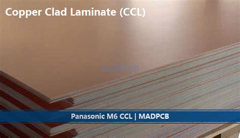
Copper-Clad Laminate (CCL) is a crucial component in the production of printed Circuit Boards (PCBs). It is a substrate material consisting of a thin layer of copper foil bonded to one or both sides of an insulating material, such as fiberglass, epoxy resin, or polyimide. The copper layer serves as the conductive surface for the electrical circuits, while the insulating material provides mechanical support and electrical isolation between the different layers of the PCB.
Types of Copper Clad Laminate
There are various types of copper-clad laminates available, each with its unique properties and applications. Some of the most common types include:
-
FR-4 (Flame Retardant 4): This is the most widely used CCL in the PCB industry. It is made of woven fiberglass cloth impregnated with epoxy resin, offering excellent mechanical and electrical properties, as well as good thermal stability and flame retardancy.
-
CEM-1 (Composite Epoxy Material 1): A lower-cost alternative to FR-4, CEM-1 consists of a core made of paper or cotton fabric impregnated with epoxy resin, sandwiched between two layers of fiberglass and epoxy resin.
-
Polyimide: This high-performance CCL is made of polyimide film bonded to copper foil. It offers superior thermal stability, chemical resistance, and flexibility compared to FR-4, making it suitable for applications with extreme operating conditions.
-
Aluminum: Aluminum-based CCLs are used in applications that require excellent heat dissipation, such as high-power electronic devices and LED lighting.
-
Flexible CCL: These laminates use flexible insulating materials, such as polyimide or polyester, allowing the creation of flexible and bendable PCBs for applications like wearable electronics and flexible displays.
| Type | Core Material | Properties | Applications |
|---|---|---|---|
| FR-4 | Fiberglass and epoxy resin | Excellent mechanical and electrical properties, good thermal stability and flame retardancy | Most common PCBs |
| CEM-1 | Paper or cotton fabric with epoxy resin, sandwiched between fiberglass and epoxy resin | Lower cost alternative to FR-4 | Low-end consumer electronics |
| Polyimide | Polyimide film | Superior thermal stability, chemical resistance, and flexibility | Extreme operating conditions |
| Aluminum | Aluminum | Excellent heat dissipation | High-power electronic devices and LED lighting |
| Flexible CCL | Polyimide or polyester | Flexibility and bendability | Wearable electronics and flexible displays |
Manufacturing Process of Copper Clad Laminate
The manufacturing process of copper-clad laminate involves several steps:
-
Preparing the insulating substrate: The insulating material, such as fiberglass cloth or polyimide film, is treated with a coupling agent to improve adhesion to the copper foil.
-
Applying the adhesive: A thin layer of adhesive, typically epoxy resin, is applied to the insulating substrate.
-
Laminating the copper foil: The copper foil is placed on top of the adhesive-coated substrate and subjected to high pressure and temperature in a lamination press. This process bonds the copper foil to the insulating material.
-
Cooling and cutting: After lamination, the CCL is cooled and cut into the desired sheet sizes.
-
Quality control: The finished CCL undergoes various quality control tests, such as visual inspection, peel strength testing, and electrical resistance measurements, to ensure it meets the required specifications.
Factors Affecting the Quality of Copper Clad Laminate
Several factors can affect the quality and performance of copper-clad laminate:
-
Copper foil thickness: The thickness of the copper foil determines the current-carrying capacity and the ability to create fine-pitch traces on the PCB. Common thicknesses range from 18 μm to 70 μm (0.5 oz to 2 oz).
-
Copper foil surface treatment: The surface of the copper foil can be treated to improve adhesion to the insulating substrate and enhance the bonding of solder mask and other coatings. Common surface treatments include brushing, electrodeposition, and chemical cleaning.
-
Insulating material properties: The choice of insulating material affects the mechanical, electrical, and thermal properties of the CCL. Factors such as dielectric constant, dissipation factor, and glass transition temperature should be considered when selecting the appropriate insulating material for a specific application.
-
Adhesive properties: The adhesive used to bond the copper foil to the insulating substrate must provide strong adhesion, good thermal stability, and chemical resistance. Epoxy resins are the most common adhesives used in CCL manufacturing.
-
Manufacturing process control: Proper control of the manufacturing process parameters, such as lamination pressure, temperature, and time, is essential to ensure consistent quality and performance of the CCL.

Applications of Copper Clad Laminate in PCB Manufacturing
Copper-clad laminate is the foundation material for the vast majority of printed circuit boards. Its applications span across various industries, including:
-
Consumer electronics: CCL is used to manufacture PCBs for smartphones, laptops, televisions, and other consumer electronic devices.
-
Automotive: Modern vehicles rely heavily on electronic systems, such as engine control units, infotainment systems, and advanced driver assistance systems (ADAS), all of which require PCBs made from CCL.
-
Industrial automation: PCBs made from CCL are used in industrial control systems, sensors, and actuators, enabling the automation of manufacturing processes.
-
Medical devices: CCL is used to create PCBs for medical equipment, such as patient monitors, imaging systems, and implantable devices.
-
Aerospace and defense: High-performance CCLs, such as polyimide-based laminates, are used in PCBs for aerospace and defense applications, where reliability and durability under extreme conditions are critical.
-
Telecommunications: CCL is used in the production of PCBs for networking equipment, base stations, and satellite communication systems.
-
Power electronics: Aluminum-based CCLs are used in PCBs for power electronic applications, such as motor drives, power supplies, and renewable energy systems, where efficient heat dissipation is essential.

Advantages of Using Copper Clad Laminate in PCB Manufacturing
Using copper-clad laminate in PCB manufacturing offers several advantages:
-
Consistency and reliability: CCL provides a consistent and reliable base material for PCB fabrication, ensuring uniform electrical and mechanical properties across the board.
-
Design flexibility: The availability of various types of CCL with different thicknesses, insulating materials, and copper foil treatments allows designers to choose the most suitable laminate for their specific application requirements.
-
Cost-effectiveness: CCL is a cost-effective solution for PCB manufacturing, especially for high-volume production. The use of standardized sheet sizes and the ability to process multiple PCBs on a single panel help reduce material waste and lower production costs.
-
Compatibility with standard manufacturing processes: CCL is compatible with standard PCB manufacturing processes, such as drilling, etching, and plating, making it easy to integrate into existing production lines.
-
Excellent electrical properties: The combination of copper foil and high-quality insulating materials in CCL provides excellent electrical properties, such as low dielectric constant, low dissipation factor, and high insulation resistance, which are essential for reliable PCB performance.
-
Mechanical stability: CCL offers good mechanical stability, allowing the creation of PCBs that can withstand the stresses of assembly, handling, and operation in various environments.
-
Thermal management: The use of thermally conductive CCLs, such as aluminum-based laminates, enables efficient heat dissipation in PCBs, which is crucial for high-power applications and ensuring the long-term reliability of electronic components.

Challenges and Future Trends in Copper Clad Laminate Development
Despite the many advantages of using copper-clad laminate in PCB manufacturing, there are also some challenges and future trends to consider:
-
Miniaturization: As electronic devices continue to shrink in size, there is a growing demand for thinner and more compact PCBs. This requires the development of thinner CCLs with improved electrical and mechanical properties to accommodate smaller feature sizes and higher component densities.
-
High-speed applications: The increasing use of high-speed digital interfaces, such as PCIe, USB, and HDMI, demands CCLs with lower dielectric constants and lower loss tangents to minimize signal distortion and attenuation.
-
Thermal management: With the growing power densities in electronic devices, effective thermal management is becoming increasingly critical. The development of CCLs with higher thermal conductivity and better heat dissipation properties is essential to ensure the reliability and longevity of PCBs in high-power applications.
-
Environmental concerns: There is a growing emphasis on the use of environmentally friendly materials in PCB manufacturing. This has led to the development of halogen-free CCLs and the use of recycled materials in the production of insulating substrates.
-
Flexible and stretchable electronics: The emergence of flexible and stretchable electronics, such as wearable devices and flexible displays, requires the development of new types of CCLs that can accommodate the mechanical deformation and bending of the PCBs without compromising their electrical performance.
-
Cost reduction: The constant pressure to reduce the cost of electronic devices drives the need for more cost-effective CCL solutions. This includes the development of lower-cost insulating materials, the optimization of manufacturing processes, and the use of recycled materials.
Frequently Asked Questions (FAQ)
-
What is the difference between single-sided and double-sided copper-clad laminate?
Single-sided CCL has a layer of copper foil bonded to one side of the insulating substrate, while double-sided CCL has copper foil on both sides. Double-sided CCL allows for the creation of more complex PCB Designs with interconnections between the top and bottom layers. -
Can copper-clad laminate be used for high-frequency applications?
Yes, certain types of CCL, such as those made with low-loss insulating materials like PTFE (polytetrafluoroethylene) or hydrocarbon ceramic, are suitable for high-frequency applications. These materials have low dielectric constants and low loss tangents, which minimize signal distortion and attenuation at high frequencies. -
How does the thickness of the copper foil affect PCB performance?
The thickness of the copper foil determines the current-carrying capacity of the PCB Traces and the ability to create fine-pitch features. Thicker copper foils allow for higher current-carrying capacity but may limit the minimum trace width and spacing. Thinner copper foils enable finer-pitch designs but have lower current-carrying capacity. -
What are the environmental concerns associated with copper-clad laminate?
Traditional CCLs often contain halogenated flame retardants, which can have negative environmental impacts during production and disposal. There is a growing trend towards the use of halogen-free CCLs and the incorporation of recycled materials in the production of insulating substrates to reduce the environmental footprint of PCB manufacturing. -
How does the choice of insulating material in copper-clad laminate affect PCB performance?
The insulating material in CCL determines the electrical, mechanical, and thermal properties of the PCB. For example, FR-4 is the most common insulating material and offers a good balance of properties for general-purpose applications. Polyimide-based CCLs offer superior thermal stability and chemical resistance for harsh environments, while aluminum-based CCLs provide excellent heat dissipation for high-power applications. The choice of insulating material should be based on the specific requirements of the application.
Conclusion
Copper-clad laminate is a fundamental material in the production of printed circuit boards, serving as the foundation for the vast majority of electronic devices across various industries. Its unique combination of a conductive copper layer and an insulating substrate provides the necessary electrical, mechanical, and thermal properties required for reliable PCB performance.
The availability of different types of CCL, with varying insulating materials, copper foil thicknesses, and surface treatments, allows designers to choose the most suitable laminate for their specific application requirements. As electronic devices continue to evolve, with trends towards miniaturization, high-speed operation, and flexible form factors, the development of advanced CCLs that can meet these challenges will be crucial to the future of PCB manufacturing.
By understanding the properties, manufacturing process, and applications of copper-clad laminate, engineers and designers can make informed decisions when selecting the appropriate material for their PCB designs, ensuring optimal performance, reliability, and cost-effectiveness in the final product.


Leave a Reply