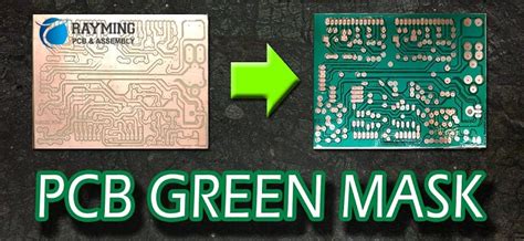
What is a PCB Solder Mask?
A PCB (printed circuit board) solder mask, also known as a solder resist or solder stop mask, is a thin lacquer-like layer of polymer that is usually applied to the copper traces of a PCB during manufacturing. The solder mask serves several important functions:
-
Insulation: The solder mask electrically insulates the copper traces from accidental contact with other metal, solder, or conductive bits. This prevents short circuits and ensures proper electrical connectivity.
-
Protection: The coating protects the copper from oxidation, corrosion, and physical damage that could occur during handling and soldering.
-
Solder Control: During soldering, the solder mask keeps the molten solder contained to the exposed metal pads and prevents solder bridges from forming between closely spaced solder pads.
-
Aesthetics: Solder masks are available in different colors, with green being the most common. The mask color provides contrast for easy visual inspection and also gives the PCB its distinctive look. Other common colors are red, yellow, blue, black, white, and purple.
How is Solder Mask Applied to PCBs?
There are several methods used to apply solder mask to PCBs during manufacturing:
Silk Screen Printing
Silk screen printing is the most common method for applying solder mask, especially for low-volume production or prototype PCBs. Here’s how it works:
-
A fine mesh screen is coated with a light-sensitive emulsion and the solder mask pattern is transferred to it.
-
The screen is then placed over the PCB and the solder mask ink is applied using a squeegee. The ink passes through the open areas of the screen onto the PCB surface.
-
The ink is then cured using UV light to harden it.
Silk screening produces a thicker solder mask layer (typically around 0.001 inch or 0.025 mm).
Liquid Photo Imaging (LPI)
LPI is a photolithographic process that is well-suited for higher-volume production. The process involves:
-
The entire PCB surface is coated with a thin layer of photoimageable solder mask.
-
The mask is exposed to UV light through a photographic film with the desired solder mask pattern.
-
The unexposed areas are then chemically removed, leaving behind the hardened solder mask on the desired areas.
LPI produces a thinner, more precise solder mask layer compared to silk screening (typically around 0.0005 inch or 0.012 mm). It is the preferred method for PCBs with fine pitch components and high density layouts.
Dry Film Solder Mask
Dry film solder mask (DFSM) is a variation of the LPI process. Instead of a liquid photoimageable coating, a thin dry film is vacuum laminated onto the PCB surface. The film is then exposed and developed similar to the LPI process. DFSM produces solder mask layers with thickness and precision similar to LPI.
 ILPIHJXb90bt3fvnA+6a0+CAB8qnG3PVRtwufouT+Nc03qWkO3AAnPCAHce4BOCfqct+H41xepySTXksjHghRGvPyxj7oIPfv8AjXQ6xdtBbbIv9bMSFGAcRhcscHjAXH/fVcm7vIzO5JZiWYnqSa0prqJiIrOwUcZ6k9ABySfpTmYEBE4jU8Z6sf7ze9WLKe3tJrae4tUuovMzJbyMVWWJeCpYc8n+VMQLLPJIkaRq8x8mMklFZySq5POF/wA9a1JGBEjAaQZcjKx9OD0Lkc/h/km+aVlXaXAIxGgO3HoFWn3UDwMm9t5kBYtg8tnkc1JbyrAdyIWLwluW+9jquOnFTe6uh27l95UtwiRwH5lDfLtRVB4wxPes26REuG5BjcrJwRwG5IpXuJrs+W+0KfuAcAOOQcn8qW5tzEYixw8gHmAggK/qOOhGD+NTCNtWDdxf3jjYse8I3lumScZPDBicjNR3Fs8BVjyjjPUEqf7rY4zWjbRq9tO8bp5qbAWXowX5ckHk44qK8li2R5Pz8bo+c7G+8D9O30/McnzWBLQoqzSIYdzZ4KcnDbf4CP5f/XqKlYFGIB+6QVYdx1Bp0mCVcdJF3Y9G6N+taCNjQ5pPNmV8mJwgY9wQpXH5Z/Kug5zyfXcff7jEfjtauJt7p7Z96AHlCd2f4WB4wfw/GuzjdHjSVTuR0DZzklduD+hB+ormqxs7mkWVdShjntpFKYlLIRIMkplsNgDryD+dYd7ZmwCiNy4Dq8pOBlc4T5fru/z16dslXyPmw2QCRk/cIyCD12nr3rntQW/mtRNKY/JGxkSNMkD5sl2Hcf593SbvYUkVI3gRGD4PlSNHgnhoJhjjvwcHgVajcvFB1DhGtmYgg+bEfMjY55zj+VZ0b4eI7Q3mxeURwDk/JwT0I4qZZWDSIwZZEeHI4AEykrk/pmtpK6sStGPDgSzKEPlzAzBT/CCNrr+f8qlglVLiwkLc71Rxn+JDgMR7gn/JqrdN5bQyfKRvLFFJU4cZK88/Xiqq3jRqyqgJLA5fnoTt5AzkZ9aLcyTDujuiR6j86N6Dqy/mK4Y3mqlirPIDnGDwRTZZtQGN0jnPoTWN1exHsHudyZoB1kT8xTTd2i9Zk/OuADXbMctIQe2TQRLjBEh59TQHsfM9Aju7WVtkcqs3oDU9cfosJiuo3BPzdQa7E1KknsRUp8jsM70knMcn+6aXvQ/3H/3TVGRwEnF1J7TH+ddxDzaL/wBcv6VxUqE3c/tL/Wu1tubSP/rn/SpR2Yj4Ys4j7t7N7SN/Ougtz88P4VgSgrfT/wDXU1v25yYPqK4sT8SZ7GF/hM3Zv9RJ/uf0rCibMf4mt+UfuH/3P6Vz8Q+RvZm/nSxmyZy5ZvJGZNkSyYGcmo8Seh/KtxIYj8xUZNSeTF/dFeW8Wo6WPU9k31IhBdNyAMVHcwyxx73AIzitWP7q/j/Oob1d1u4/Gvalh4JXR4tPHVJTSZVsYo5SC3YZFQ61GAbcgYAOKs2HysPpima1/qY29Gp0taY6ztiS9pzZt4/oK0Nvy5rJ0ht1uPY1sHGyt47I8+ovfZBXM64FN0ucfd7101ctr+PtS5z9w9KohGY4RBkMMkdKh+zlgHbPJ4xUyLE6E4JPrRtYYAk4A6Ur22Ki03sItmChf+EHBHeuk8EN9k8QWLKSvnJNbtz1DoWH6gVzuQVwJDyeRU1ncPa3EM0b/vYZElRs9ChzR73cu6PouCeOVFJIDY5z3NT/AC+1YFlcpNb28ykbJ4kmTHTDqGq9HLk4H4mtlU7l3NDIzjvS1XQkgsOg+Uf1qTJVRydx9a0UrjuIyx5yAwPfb/hXmnxHcnVPDMXzYWG4k59TIq/0r02ORXyO4rzL4jj/AInXhw9jazAfUSg0paq4I5s57H19RVG+P7609vMJ69AFJ61ePTt39azr7/W249Ypx+JXFcdP4zSWxm06QkFMEgiJAcZHb2q19t1KO30+POILG5kntN0aYWZtrtkkZPY4NSrqmoRy6j5YgZtTCCffDGxJYA/u88CuwyNWyuYY4wPPDSeVGZ/PYHIKgn51+Yfkep/Ge21bTbr5TJ5bknKTYXOck7W+7zgAdOtY88N1qM5ubnyY3ZEUR2qAlgq4GAvGfWkt9DvZTunxbxdcSENLtxu4VeM46ZI6Vg4xe7LuyLU71ri6uMEFAvkKw7gNuYgjsT+gFZ2RVkFrG8UskcjW04OyUZjfacjcPQ1MmpBJtTnNlaN9ujkj2MnyW+853RDsRWi0WhO5Ul4ZV7KiD9M1csUffGwI2JGxbpktJ0469v096pS/6yT3YkfQ8itCyA3u27/llENmONpHBz+f50qnwscdyW9j8yBiB80Z3j8OCKr6dFHK6xuYySGePkEpkbec8cnFaPHIPQ8fUdKzIc29wU+YhJMhQgI2t0dm64HFZUXdOJUl1GOhgncYVFzlGKFsY5wo9e1adzEl1b27HaDhUO3dlSBlSd3qOD9PyL5VCPcFCykCRCAyhZc7TjB7HNLp7I0Lxv5uPvBTgtuyWDMzY9/z61q3dcxHkQadIVkdJN5BzFIxVSAPulUA9ufw/OvqkRieIMpDgOpOOCAc/wCfrTWkW2uZnDlnDgrg5BVsEjI7/jTr26+0oB3TZJklmJUjGcsfpniq63EUnOUiJ64ZPwU5/rTSf3K/7MhA+jLnn8qVjiJPd3P5ACp7JrBJYnv45JbTzQJo4W2ucIxGDVAVFbaytgHawOD0OD0NdTotysttJGu4mCQhFP3jGcsBjJ7bh+ArBjfSPJ1ISxXBnZkOnlWGyNdxyJR9MU20XUyLk2Pm/cUTGE4YqDuAHftniokuZDTsdfJNbxYSWRA+PuA5cqBtJCjnkY/xrD1DUEEU0CKvz7wh3fMu77xZR0PJ79/asmGC7mkkSJX81VJkySrAZwdxPNWRb6dHBZm4Nwly88gnGBsES5GVx+FQocruNyuVD9yH23r+Oc/1pyciY852D6/fWp2FgLecAymXzCbQ9MpuCneMY6D1qNzbh7gW7SNF5abTMAr53JnIHHWtU7kky2cMiI7K5dlBJ3HkmobqzhjgmdFfcBhcnIyTiul0jRdR1MQJaWzSYjQtIcLEhI3fM54rsrLwDYqqNqtwJFG1mggyqkjna0h5x9AKwjzt+Rq7JGdr3hqKbTtP160i+Z7G0kv4lA/54r++UD/x786410tlBZlGDwK9xM1pHEtuiKYVjEIjAG3ywu3bg9sV4tqtna2094YSzQJcyiAZyAgY4FYYnljJNPc0pe8n5FIi2XLbQAB3qu15ZgZ2jg1aitY71TI+8Y429KoahYw2+zYDg1jTqQc+SW5pKm1HmWxPZ3sRuYwqHlgMgV2A5VT6gGuQ0eNWmWJQCxOcntXaJA4UBuMCumCfM0loclaN4pkBFKR8rfQ07adxA9aVlIDA+hrWzRytNHBzcXlyP+mldlZ82kf+5/SuOuuL66/367DT+bOL/d/pWUd2dlf+HE4y6GL+4H/TSte3ODD9RWVffLqNx/v5rUgORCfcVy4jdHq4T+H8jpnGYD7p/SudiHyyj0dv510fWH/gH9K52Pjz/wDro1LGfAjly345Isxg7Qam4p0EDPCHzxR5LV8/VoyTvLS56qrQbaWth8f3F/H+dNnGYZB7Usf3V/H+dLIMo/8Aumvrnqj5WDs0yhaHDJ9adq65tSfQ1Dbt84Ho1W9SXdaS/TNcuH+Bo9HF/wAaLK+iN+6cehrZ3HpWDojf61a3QCa6Y7HDWVpsBzWHrFqZJA4PIGMVup1qGeASSZx2qKkuVXOOvU9nDmOQSBIwVMhG48jFDadOZUSAl94z1rqTptu+4uB0zkU7S7GNpurKAxCmpVWyuJVtE2tzmm0S+QeY8RC9+elRw2LmUgg4UjOe49q9HubNZIzArMfr3Ncje291BLIrfLtbC46kds1rTqc6fc1qPk16HoXhtHk0q1hjzm1/dAHr5Z+Zf8PwreGIxsBycZY+privCN5dJJI0xP2d4xCwU4PB4I+ldqfLZQ8fKnnPr7k0RaenU3py5o3J7WViJU7KVP4GrexsjPIJByKyYpDFNkdSAOe47irNxq1natHDiWa4fBjggUNKVJ+8RkAAe9bxkkveNUruyLjxyFw6sBt49tvpXm/xNPlz+GbsAMF+2R8HGSvltjNdlP4hFrIqXWm38aF1UyoqSxqp/jJQ5+vFYHjyLT9Q0ew1BT5kVrfIHaFg22OQFG4XjPTjIpqcJJ8rKcXHc80/tByqubdghJUHzO/XHSkufNd7aWSNowrFcMdxJLYJyBjg8HmkltxuuY41YIeYVcBW+U5ViFO3JHXmpUPmQqdzMYkWaIMSQoziQBenXk1HLGNpIV29Cv8AvZ4fLUDJC7xnLNLEGGQSe4z+VVjsLW5cExlEDYOCQCVNW2Bgmu4AobzCk0DA7QrD94CCfbIqtMEIDR/dDEY9N43YBPbrWpJ0emFIXlt1+UMqvC3ORjC4BPPB2kfU/hpfMANvUkFfYkl1/XI/GsLTxaw+S7sXMqgCViSVV1wUwM9OfyrdySSTxnOT6ZOCfwOD+JrilubLYwNchSNxMq/JOiKCB9105TJ9xkH6VhV2V9bpdW0qsOeJFAwCMNnAJB7gj8a5GZBFLKgOVVjtPqvUV0UndGctwk58t/7yD81+U/yqe2l8toXJwozDIfQHlT/n0qBPnVo/4gS6e5xyv4/0pEYKSGyUYYYDrjrke4rRq6sSaMuoQrkRguenov5n/CqZn82UPL8o4GEHGAcjdnPH4GoHQoQDyCMqw6MvqKSojBR2KbbNZr9ZbcRHndmIbi23dt4IHv6k/h656SyBkDMdoypBx34JOfSnQQyy7lCkKwBDtkKrLyDn8xRdRGKXBOQ6hsgYBPQ4Bqk0nYQhTzXi8xiDv8mRsZIPY/59Knnhit/JO5yu10xjJYHtngf59qlX/SLIqANwGOAB86dCcetQyXRaGMugDDa0eTkswGN+PSo5m5aDtZFSXjYndFw3+8eT/hQw2xxL/e3SH8eB/L9ans5oEF6s1rFP51uyLJKTm2Oc+amP4uw+tV3YuxOMZ6D0A4ArUkSMIzqHOFzlj7DnA/pXV6bbC1tUDLhpcyyAdRn+HPX+6v4msXS7AXEkUjc4cMqdmCnHzexOB/8Aqrp8/wBw+mCf/HSf/HnP4Vz1pdDSCGOkbEu4BcAgyqdr+/zDsT+i1z+rJIyW85kUrl1jUrtcqTkMxHBJ+grflVHjaMu0auNu4LuZeMAEfT+fvXN6q109xHDJsARQIvLztYNxvweRn0pUtwkUW4ES+kYJ+rEmmkMI5WH8TIo/DJIokILuR90Hav0XgVet4gsNtIx+aRpZNp4/dLhd+fzA4710N2VyLHYaN45ttJ0u0094GcwKwDwPGu/cd2W3HOe1Ol+IF9cyxW+m6aJZ5pFjVZJmkbk4zsiGf1q74f8ACfhW6s7XUNQhe6uLhfMMCuyQwAkkIwjIyw75P/1+us7Pw7pQZrDTrS1JGCyRqHIHq55/Ws1bqxsqX1heXWjXytKyXhh82JoyUG9BuKcc4PTrXlsqXcke1iTjrgV6pqGoSzRSJb871KF+wB4O0VzjaQjISpwT2rgrTg5K3Q2p8yRxSpcW8fmBmwe1MnglmiDsCfSu3/sa3lhKsQGA4+tRJpdqIijnkcCsrq97amnNpY5PSbKWK4huM8FgCO9d+kIZB8vYVk2lrbQlg/VWyM1sPetDCrrGCBgV2UayTakYVI6XRSeMKx46Gqsy4J9xU76i7kny1qCW4MwwVAx6V0SaZyykmjgL/jULr/errtMObOH/AHa5LUxjULj8K6vSTmyi+lYLc6a38KJyepDGpzj1IrSt/uxexFZ2r/LqcnvitC3IKJ9RXLiuh6mCd4HTL/qV/wBz+lYC8Nc/77V0EfMKf7n9KwAMS3Q/2zSxf8NHLl2lWRs2XzW61a8gVVsP9QPrWjkVNSkqkYsxdR06s0n1JV063HAXpTxp0G1uOoNWQyjqy/nSrPCDy6Y9zXsWRyHCuohvJo/7spH61oXShrWUeqf0qlqJT+07oqQVLggjpWg/zW7e6f0rzaStKSO7Fa8kjD0f5ZnFdInK1zmn/LcsPcj9a6OI/LW8HocuIVqg1fvVJg9cHHr2qP8Ajom1GKFVtnxknj1rOum46Hl4yPNSaJDC0oZQrYHUgHmpbQmCVAEPBGFPU1LCbpkQoMBh6c4qKRLqMmXy2ZgeAtcdnscboNRTgndFy4e4aUbiUPBAHpVO8tBcqWABkHzZ+lWFW+lkimZfkUYfd1FSyxXErrGihFByXBHI9K0i5LqbujWqtyk7FfSLW4t0LlwQ3JT0NbtjqM8b7dgMZPzKxwPqDVaK1RcjzSBj171FHAjTMTL+6xtxk5zQpa83U6oqslFL5m/PeWDhVDlJDyBjofqOKxSwtNYndpObyJHVyc9OCoJ7VIbaywgEnI5yTmqur2qzwJJBJma1BdR/eTjcAfXvTqVHNWZ6GGnKNT37WOot50uYUGQXGVP1FYesaJJPbai1kqq0kMstzEhKiYphwSnTdkcH3qnod+4dYkDO0uBtHJLewruYdsaqZMeawGQvOPanhouU79jurNRjY8PaAr5WeqYh3YH3XAaJ/wBcVVt2Cy3cYXBikaYKR/CPllUD0xz+H5+x6v4X0vVRNIo+z3UiFTLEBtc5JBdOhIPevMde0bUdCvra4uIspJgNLHkxSkfKwB68jsa9Tk0aexwPuZGoRAwQuo+a2P2eT3iPzRt+XFUVcPEINvzfOUbPXHzKuPz/ADrZaEMxhzlHX7NkZ+ZGG+F/5CsIqyMQeHRiD7MppRemoPctR/a826QsZIgqThCVAA3fMrEe+RXUwTpPCsgTYjZG0dAANrAfhg/ga5OOUQTJOo+RwxKj34Zfwrbsb5v9HBh2wyEqHZgctlsDHoeQfrWVWL3RUWax9M45O4jseEY/ntauT1K18m5uiOAWWULgYCyEg4+h4/EV1nABPLdvcgLggfVcf981i6+kRjgZpE+0I+Cm4b2U8E7euDw341FNvmKlsc+uSygHDFlCnOMEng5q3e2c1tM8Umzz1VZJEjOQQwzuX+o/p0ZFcQR2l3bvaxySzmMx3DEh4QvUKPeq+SCGBIIPBBOQR71063MxUkwCrANGTnaex9VPY07ZG33JB/uy/KR+P3f1pSY2wZBhiM+Yg4Pb5l/wqa4FrIlmLOHa0cIW5bztxmlz98K+CBTAsWbPHEySDAU5TkHIPOBg5pt5skCDcoZWyGZlC4PXnP8ASqPlTf8APKT/AL4b/CgQzf8APNgO5YbR/wCPYrP2a5uYfM7WJUm8hWEblyxyTjCAjjIB5P6VDiWZyc7mPLMxwAPUn0p22NfvyA/7MXzH8WPH86RpCRtUBE/ur392J5NaEk1zbXFrHbB42SO4QTRu2B5w/vAeg7D/ACK6IXYKMdzk9AAMkmrVtPaFmGo/aZokt3jtlRz+7fqvU9KTT7d7m5jiAJXBaYDvGCMg/XgfjSu0tRm9pFv5FqGbIkn/AHjeoQjIH5fq3tWge4PB53Af+PAfooo6YUckYA98HA/M8/QVHJLHFs3sRu+4yqWIxyG2jPux/CuJtydzbYzdQvore4t3CvKqq4lHKKsuf4W5B/8ArVjTvK09xcSjaxAdVyDt8wfIOPQc/hV7Urq2EBt7eRH3Oc7OQPU49e1ZUpPCMcsCWkPXMh/w6V1U42RlJ3YkELTyxQr1kYLn0Hc/hWswj3uRzCgAUesEPyqv/Az/ADqtZRlY2l6NMTEhP8Ma8u4z+VOuZGP2e3hJEkzJJ8pxtUfLEvB9PmP1/JvV2DZXFha9VpZIruaIySNEnkyOilyd0knykdOgrvvBuk3kon1nUJ5ZYLi2nhs1mmd2C7gDJsYkDOCQfeuE2oONx8pFZN3pEnzSv+PT8fz9J0V7+30LToJ1O94jJ/d8qKUl1ix7AisatWNP3pehUYuWiLv2cK4O87OoFSGCIMHzwecdqaVlKrtTPHc08pNsACjPvXkfWIrdnT7N9hrQwcOO/YVBLFbsN4HI7CrPkzbcDaCaq3JjtVTzplQyMFBOAMntzS+sQ7j9lLsUpViJ3bfunpimSOJbeVMY2jirj2rFMh87uciqywCISAsSSDwaz+tU7qzG6MrPQx6UUrDDMPQkUgr3DyGjidWGNRm9xXTaOf8AQ4657WF/4mDn/Zrf0Y/6ItSn7x21F+4izm9cGNRz7VctOY1/CoNeH+nKf9mpbI/IPwrmxOx6WB+BHWQcwR/7tYDD/SLof7Rret2HkR/7tYrD/Srr61OK/hI5cDpXkjV03HkfjWjx6Vl6a2ImHvWjuroo600cWK0rS9TJEkpAy7H8TS5c9z+tEYyRVjatbGBgThhcyfga2k+a3X3T+lZd6uLo47rWrbkG3T/dxXLT/iSR6OI1pQZh23y3bj/bNdDF0rnkIW+kH+3XQxEAVtT2ZhifiT8gI+eqF3amWYz5AEIDc+3NaBxuzWXrl1sspY0AVj1YHBxVu/Q4+VS0ZYt/EKPJ5CyKNijntVr+2I+84/AV59aSbZOTjNafmxL1dRx61DooVbmpy5Ujrf7ZjCsBKxQnLYFRnW4R0aQ9utcyLm3Eb/vF496ga+tB/wAtBQqMTHnqPZHWf27H/dc/UmmnWvL+7D975uTXJjUbQsBv5PFSXWpW0JRclvl7U/Yx2sP96+h1A1+b+GJR9aR9cvJY3jwqgqeR1Fcd/bMI6Ixp8espk5jPQ4/GqVFLoUo1mey6DZ2dhaQ3Ebie4uIlc3BGBtYZ2xjsPWt2GXqx5Y9z/IV474J124g1CWxnkY2d1lkDEkQS54K56A9DXqqPjFEfcdjvld7mukpPIH1pt7ZWOp2s1peRLLBMuHVuoPZlPYjsaihdcDP4VP5gB4NdMZEJnkes6LcaNcfZJGLR42W85AG+PJaJz2ypyp/D1rm9RTc8d0FCi5B3gdFnT5XXj8/xr3HWtMh1zTp7UtslIL2sh/gmUZVjjt6145qtre6fNc2N/EsTeYruOWAYjb5kTHGR36d6La3XUroYqEMDExwGOVJ6K/QE+x6H/wCtViK6aGAwMjB1lLI2cbD1575BGarOrIzKw5H5EHoR7U4fvgB/y1UYX/poo7fUdv8AORq4jfu7+EQMpuXDSRYi+z5QZGcEEZbg+p71h21rPdTQKFfbLLtaQglePmb5j6CnLestjNYeTAUlnSczMn75CoxtVuoHrXSWUlp8nlMgVVCQBAyozNgyFCMHsBxmsn+7WiK+J6kFzo1hJ+8iHknPy7cFD07E7D+YrIu9MvINxEAZMZYw7jjB67G+Yfr9a6vplvX72CB7csox+a03HTjg9FwPzCk4/wC+WH6VgqjW5fKcQ8U0YUuhCsMqeo/MUyuxuLK1uVZZE6nJKEhgfU/xfmD+lY9zo0qRkwbJVH3WLbHHU4J+4f0rdVUyeVlK1kVLbUt1l9o3xIqzkv8A6Id2dwxxzVLcSACSRnPJ71MJb+2FxaAyxC42rNFtIL46DBGfyqzaaTezfM8G0cFTMWHHrsX5v5Vd7askogMxAUEsegAJP5VMtpeMyoIJSxwcAdF9Sen610Fro1nARK7vK4zznCLnI6KcfmxrSVURQFUKvbGPpwWGPyU/Ws5VktilEwItDeTa0rCJB1AYOx+rHCj8M1V1Oz/s+eLyGcRugZGJIYOpweeD6EcCuqHHPRj0Pzbvw6v+gqtdRwNGjSqh8mTfh9vAYeWxxyM8jqT0rONV31G4oy9N1NyDHdXKnlVQSrhtuMcSjv6Zqe6vraN7jc4EixgRoMk7XXd8rKMc8D8Pes24XTYHv0ljaSaRP3HlNhIJP9rnv16fzqgEKljLwqHBwQS7ddqkcfWtuRN3J5nsODEbp3++7MYx/td2x6D/AD0qNEeWRI0BLyMFHrk96R3LnccDjAA6KB0Aq3aqYyx+YSuoAKgkxo/BPHOSP0+taPTUkvOYFCheLeKPywe5ij5kf/gR4H4VUt/NlluLt1Ikkby4AcjDP3GeyiiV1kZYVP7tyu4AHiGLkA9+TU+5TyW2rzGp6bc/NI4HsOBWauo36srd2LmnwWtxe2UFxIsdqzCa4ZyB/oluc7cnvI36Cut1bxHpwgbyZgwWRQTGeAAfavKLuZrmeR1JWMfJGo4AReFHFT2pkEMsKjIc59646+DjWmpSei6HRTquCslueqHxj4dhSEPdjcVGQOSD74qNvHXhgZBuGJ9lavKbi2whbGGHWo7OAvJvYcD1rlWUUErts1eKn0PT5fiHoKEhFmf0wh/rXN634v8A7Whjt4IWT96jhm6jByMVgvaRuc7cH2qukXlzqp4AORmtqeX0KclJXbQe3nLQ9Rs9bkFnbK4XeI1ySfamPqili5ZckY61w4kmOBubHbk07Mp67vzNH1ShF35TLmqy3kdU13bksS65PNN+22o/jFc5GSPvZqXKGtnO2liVhU92VNVcTXu+PlcYzWtpt3Fb2uJM5Has1wm6pIsKCDyDS59bnTKivZqDKer3CXVykkf3QMGp7JgFA71BdQozZXg1LZnAx36VlXalE6MLHlVjWXVHiQIEzjvVeKczSTyEYJ7VAxwTTYGO+UdKivd0tTPDxjGs7FtL6eDcsYBBqT+1L32/M1UXG5s1J8npWtGVoI58TRTqtmqDjpUm4+tQjIOKeDXUeWUL3/XKe5FXrYkwrVO+4eI+1WrQ5iFc0NKzPQq64aLMZzt1Bx/tCujj5VfoK5y6+XUD74P610UJzGh/2RW0N2jHEaxiySqWoWkd1BMhHzFTtPvV0kVE7oP4h+daHInqedyxyQSPG4IZSR/9eoX3HnJ/Ot/xAkPmRSJt3H72KzbC3iuJ1WVgqDk571on1O9SUo8zM0K7HaNxJ7DJrTttBv7lC+NgxkBupro4o9FtsbRHkdzirP8AaVivAcYHpQ5voczn2RwE8EttK8UgwyH/ACaVg0jxDnLYUfjW5rgtbplngI3j73vWVarmeAsOEYE/hWildXNFqrmnL4dulgjmhO8lQWXvWY8E0B2yxsh/2hXYJrESKFVCcAD8qzNWu47yHAiAZTkHAzWak+pMXK+qH+GoAzzTn+H5RXq+nXRmhhDH5tikH1xwa8g0q9e0hfYASx5Fd94bvXurTzXwHgndMZ7EBgayqIbT5mzto5COPSrDMSufas+JwwVh0P8AOraOCpU96ISurCsV7PV7Wa5vbSOX/SbF1juYnBV0DAMCoPVT61Pq2kaR4gtjb3sSlwrCCdQPOgYj7yN/SuR8T6VqkF5aeJNGBN5aoIb2Fes8IOQcd/Qitbw/4m0/VET5hBdKdstvK207hwdm7r9Ov9dE+X0H6Hl+saTe6Pey6de4zGc2txyEkjbkcnsf0NZ0zQ7bdEgMUsSFZ2LlvNk3ZDYPSvWPHsVhdabayyhBcrOI4cj53iZSzAfTAP8A+uvKZ4zEyxyklcfuZgMkDrtYen+faqU03YLaXGkrL94hZezHhZP9739//wBdaw1G2s7OztShuJFVjMrAqELfME+YEce1YjqycHuMqQcqw9VIpVk4CuN6Dpzhl/3WpySe4I6qzuQ9rHJHiR/mLKG+cZORHkHjHFTx3dvIm7zI1JkaN4yyhtynB3L9316gfWuesLsWcd2YC8ssybI0zsMfHLFTnJ+lLo5DXL27Ql2nC5YrlkCHLFu+K55U92WpHS5zgY4wCFIOQCOyk5/ImjI5bOFA+dsn5QOSWYDd+amsqTUrcXItFkdUSRgzqq4aUnb1Y9PfFTTXaIkIlkjMU5cLKM4Ij5Zeh68Dr2qORofMjnLy5lmvJbhdyFXHkj7rIqcJwMV1sE4uIIJgPllRXYYG1W6EEHCdc9Sa529ie5S41BZrcxxPFFtDHzCSM5wR/n8K0NOvC8UirszGiyuXOPKB4bHHTvxj61rUV0rExZrk9OfoT/QsP5LQXUeZlgCil35IbaOO+ZD+lZkV9FLcCBLgSNLhSwyi5yc4br9eapapcxwStCiAyAl5HJIX5uQAB1HeslTbdiuZGw1wzxSNEpXAJ+cYzjDZwOMfUmqUF5ZTSTRSMFdbcussroUDYwR83HHpWfZ6ldwmV5hvheIxASMI0A9BwTj1wKzy0Sf6tdzZJDuOF/3FP9a1jTtoyXK4BFX5peB/Cg4Zx6+w96TKyMN7BFCkLgHaoHO0AUzLM38TMx9ySamSMhgoUPN2XqkeO7np+H/6q3ZI2OIgodu6R/8AVRkf+PMPT0/zmyYbm3USo5djl5lIyCe5GOfrzVqKFYdzFi0hKmRz1OfT2p5IGTz8rZz04rllWbemxqoaamTHMMvuOGkcMzZwCoyQmAM4qzKGkTy0cMjR7QwxkKTk/dOMmofIW6uHFureUD87Dp/wH61d+zyqAqR4A4FFary2tub4ehzu72KAsEUdasW8awEsFyRVj7LdHrgU+O1mGckVy/WH3O14ePYkg046gWWMpvbkhq0bfwlfKQS0QB61nJb3MTB45tjA8FTVsXWrnhr1/wAOKca8Le8Zyw8/sWsbUfhNuN1xGPwFYWuaGLN4/nRgTwy4yDUhmvz968m/76NV5I2lIMtxI+Om5if50niKdvdQQw807yasRRRKiKOCcdaftU1IBEoxu/WkLwjuPzrH2tzf2RCVFJtPapGkgHO5fzpv2i3H8a/nT9oxezXcpyh91OjEmKna6s+pZc0z7bZj+NfwqlOXYpwja1yCRJGPQ/hT7SCYE8Hr3pxv7X+E5PsKkS9Rh8tOUm1qhRSg9GNlhu1fcBlT2HWn21vcb2YocH1qpcawsLFCp3YqS01gSjaFbIonzyp25dDOHs41G76lz7JOXJ4A+tSfZZv8mqUmrOjALGSaT+2Lj/niazj7VKyRpJU5O7Lh1ODPAJpP7VQdENZwQDtQY/avQ5keP7BFyS8+0ug24xTlvZocoAMVQU7HU1NgOxOe1c70qXOxQTo8pHNMZLgSuecdqupez7QAxAFUpFUMOKmjGQOKrm1CUE4pWJmurlv4zVSZ7ps/vH/A1Z201kJB57GqUrGbpowrl3LYZi2PU1JbW7vyMjNPNvtkLOc89KuxOmAAMYrV1V0H7F2IhaerGnC1QdTWnp1rHeXAikkEceMkk4roRoXh9B+8vM/8DFEeaWtzKXJB2aOFnhjAwDUCRRKQc9672TT/AAah/eTq2P8AbzWRrcfh3yI00xQZdwyV9KGmldyNISi9FEzIxDgcU94oZFIwBkVDDFLtA2t+RqcW9yQcRufwNZc3maOn0sZCo9tPtIyhbqK7rwywZNQiX/pjIMe+VrmBpt87ZaJ8A55rqfC8EsF5OHXCyWzDn+8rBh/Wr51IzqU3GLOnd5k8oxu6krg446VPFqEwI8wKw9uG/So5S7QA5+62OnODVZeKaXc4joYrhJQGUgg8EHr9CK5nxH4XFyr6rpMYF5H+8urZOPtSD+JB/wA9B29avwyGNsjIrStr1SwBO1gePRvpVbb7AmeQzXmESSaaSRgJI0SQsXUjjaQ/THeqCTfvvOuQ/wAyqI8blTZnoCOfxr1DxP4OttZSbUNLVYtTwXkiGFiuyPXsH9+/615ybV4WMBLGRAyzwvkFHRtm1lfjPfg1UYwirlttioE2IsgRkJ3MkowjEnGUkTv+v9GSafAwzDL5bnpDc8Z6n5JR8ppywkbjbs0cuDmIEAMRn5TG/H+fzjW7WMmO5heFu5jX5D/vQvx+RFXZ9HcnQqTW88BxLGy+h6qfow4oWeZP4s8Y+bk49Aw+b9a1Y2yN0Dq6cblj/eJ9HgbDDp2qN7axlXd5bwsMhntz5sWfeM4cUcy2egWM7MDdUdSe6MGH1w3+NWp7pJ4Le3BEcUGNqiNiSQMZOCRUctm0QDCaCSMkhWV9vT+8HxiovJm7LkeoZTn6YNVYQhjj/wCe0f4hwf5VbsrwWX2gK6OJk2MpR8exJGD+FV9h8nZ9ml8/zd3mfNt8vGNu3GOvOaj8mf8AuH8cD+Zo33AVWhjZXQyllIZSNqYI5B70TXU0sjSNgyNyXf53P/An/wAKcltI3O+JRnBJcHB+i5NXI7KyQFpPNnPY8QQ/izfN+lJtLVjSuZqrNKwADyOfTLGriadJgG4lSEHog+eZuM8ItXshV42xRdtv7iLGf77fOfwqv9stVJRSz5B/1SlEJ9Cf9Yf0qeZvZDt3HGC3jR44YiHI+9Kxa4fHYLH0FVzKltIGi5icbGAUDIHIPHGfx7VLuvWHCx20R7uAu7vkIPmJ+pqtLbzHzCZZHC7du5dnUHHyk59R0ot0kwv2NHzI2QSbxsKZz2GPWs2e4Nw2xWKw8bj3bHfH8qdb2dxJHmUskB+cKern1AqdLeMYwO9cjlCm3Z3Z206Mp2ctEOivoLeNY4oyFH5k+pNKdRc/diY1OEhUAeUpI7mpA6jpGg/CuJyi9bHpKMktCkb66PSFvypBdX/aM/lV/wA49di/lR559APwpcy/lHyvuUPN1M/w4/A0D+0jznH4Vf8APJ9KQyjvT5vIOXzKBTUG/jNKLa+brIavCWMU1pZCPljbH0pqUnshNRW7Kf2K4P3pj+dJ9iPeVj+NWDI3GcgmmFjmq5pLcFGL2Ihp6sPvn86d/ZsPdiamBbHBpS+B96pc5dy1TSIBp9t3BNO+w2a8lKcZcd6aZT3ovIfKh621rscqgBHSoooxl8DvT0kJDj2pbc/6z60a21E7XMLV1C3C47rS6ZwWpdY/16H2pNN6mvQ/5h0eZH/eGXcZl6etP5pcfvPwpefSuPc71oTjGaduWqwuYR1NNN1Dz1rW7OXkXcklUMV2+tSINvLVV+1wrjg88UpugOgJo17DSila5Yc5IAqVN2B/SqHmyE7vLOfxpwuLpTwn50mn0KVrWNDDY54FM3JnG6qpnv5BjZx9Kj8q8J9KFfqJpdEW3gSTnNPjs0B++aqrb3h/jx+NPFvdd5sfjUu/Rlp+RdEVuhyXI+hxSNJp6jncx92JqqLRj96Y/nTlsYf4pCan1YXfRFgXGnDpEmfel+3WiH5Vj/KoPslovXcaPIsR/A1Hu9w94sf2tCv3Qv4CmHWX/hyB7CmCOyHSI04LbjpAPxp3iLlYf2xKe7n6Ve0PVJjq+nKyvslm8ls5xiQFearK8Y6QJ+VS2115NzbSBFASeJjx2DDNKMo3uKUG4tHpKqWjuFwDj5hVLyjk4rTj2hiD0cEceh6VG0aqSvoea79DxSoEbA4qeGEbTPKD5Sn5V7ysOw9vWrdvDFJueQ4ij+9jqx/uillcTN0CqBtRR0VewFWl1FcqC9uUcur8E524+X6AVi6rpVtqzTXDRiO5Y586NAdx6Zde/wDOt828R5xQqhSABgdBU8rTuO55nd2F3YkrcxkwqcCYBpoPUZYfvF/HNVnXdGM7JIe3mYmh9MrKvI/GvUJ7JJCSvysevHynORyK5y88O2jO0iJJazN/y1tDsDcZ+ZPun8qdreRXNc4aSziyHjZ7duqliWiz/syLyKsefNHg3MJK7sCZCWG32lT5vzzW8fDmrFm8jybgYZiYiLeUgY+8j5iP6dazriwv7T/WW88IZgjsI2CgE8lk5U9zw1Pmez1Hp0M6aaMLK4XdnYEclSeP4W2cck85FJBa2zxROyEsU3E7iKpXBijkaOMnA6jkDOTg7Tz0q5DcwLDEpkUMEAIJbOfyqKiaXulR31JTaW391u/8ZqC4treOKR1U7lwRlie4Hep/tVtz++Xv3b1+lRXc8DwSKkoZiVwATyAwPcVlFzur3LfLYYtzCDCIlJcphgqlzuJz8ob5RjpwKlVruXkAJz99x5ko78E/KKqWYSUvF5hTAMvOSMgd9g3enete10/UroJ9n0+6mLAZJidlzjnCjC8e7V0uyei1MSj9kSV2aSaWc+iHOOOjSN8v5VOkaID5Sqqj7xhAJ4wfnmfiumtfBviC4CmcW1qn/T04lkA/2YIcR/mxqXV/DOm6dppnlkuLm6E0KB7hgsSg9RHCmEH61M+ZRcmVBKUlFdTlE2sx8vLnPLRfN/31PIMfkDU/kLkMVG4ehYk/Vm5NTAqBhcADpimb68mpiJS0joevTw8YavViy4KL2wKrIOPxqztMg69AapgkbsdN2Kzh1R0b2JiDn2o5HajB47ZGaP8AgXFQjXQUN2ppJ9KX5R3o3Crv5C07jCPam5HcVIZF9KYWXnIqk2LQs28ltuUOg69TWk0lsQFLLj2rD3AdFpTKR2q7y2MnGN7l66aD7sajp1xWdtOefWlMxpnmGlys0TUUTbSRgCm+STUfmydgfwFHmTejfkaFGSByTH/Z8GlMVRl527N+VJul/utT5ZMSkkTJD97HpTIAQ0oNIskq8hWp8W8tIzDGRSaaWoXTMPV/9an0NM07h8U/WP8AWRmmaacyCvR3oHm7V2agO2UH2qbzF9B+VCW6TSYaTYAM5qf+zoP+fk/mK4Hy9Wd6diithHzlulSLZQdM81OpFPUZZcetDqyEoRKF1aqiA46MKVY4xsO30q5fD9230Bqnu+SMjrxVxlJolxSZa3EHAVcY9KME9h+VMR84z1p+TyKjVBuJlh3/ACpSSe9AVT1NOwvenzWGo3EQFu/61IIhnqKYGUHiguT0FS7saSQ59keO5PTFKiTSfdAAojfkblz9avQywJtyOD1x6UWXUmV+hnyGaHJZQwqWMxuisQAT2q1fG1k2+Q3B+9mqWAB14qZJdCoX6kuIx6UZjHcVWaSNerCjfGw4NHIyuZFkNH6imSLGwODUG9B6ml3r6UcjQuY9OsZjPZadMDktbQkn1ZV2k/pV90DyDDD5gM+uaw/Dcm7RLUk5KPPGB6BXJGa2schj02LXqxd0mzwKitJpD3IVFjT7q/q3rTV29zTS4zSgqaOZ3uTYmVc4A70u1E6jJ469uaizjgE05QCeW69zzj61ftExcpM6cA9QeQfyOKiMWeMcd8+mSKtxoAmXYYGVHuTTSNxAXqxx+fNaWEQrBHHEWVQGlwTj+6OOKqOswB2jI9P/AK1acuM4HQcD6Dio8KeoqJRTGmcxd2Fpcq/n2sDt1y8SbvzxmoovDnhyRUaXTYOQMlNy+o/hIrqpIY2U5Uc+tEVtCY049en1qNnoVcwovCHg9sE6cp7/AOun9j/fq9F4S8Hpj/iU2zf9dN7/APoTVprDGvTP5+1SrtHrwePzrVSJdyO20jQrXBttOsoiOhSCMEd+uM1eIQAAdBxgcD0qAMv+fpTvNwOg/wA4q7onUjk+fhQc9fp0Ncn4386LS7UOwG+8QAegVWPNdeLhAPlUA1yXjlhJptm5HS9Ax9Y2rKtbkZth/wCJE87EpHejzfUn8qUkDon6U0uf7grx7I94kEjcgbjmo4xIG2lec5pRI/UACneZKfm4zSt5BcmZXbGQOBTTG/8As1CWmIzupoeQ8FzSUbFcxN5T/wB4CkMJHV6FQnqzUvln3NO9g1AQqOr0vlwjq1NCAg5zS+Xx0zRzeYtewpW2GMmkza+1RmM/3aTyW9KrTuT7xJut/SlEtuv8GfwpnktR5eKPd7ivIebmHtH+lILtO0Z/KojHz1pyqc1XLAjmmPN1npEfyphmc9EpxDY4AFM2yetNKArzEMsn92npIWyGAHFNw4HIpgyXxjHFNqLQRckzI1gfNGah04/vBVjWP+Wf1qrp5/eV2x/gHLJ/vzc2kyqAcAjmp/J92/Oolz5sRx2q9k+grzZto7kkygJRUkcp3cj6VXIAdwOgYgfgadzj8auUFsLmZNctuifucVRHKL9BVp+Y3z6VVH3B9KqCsgb1LCY45p/HvUa9F/Cn81LY0h42+ppcp70wVIAOeKkY3K5yATQSx6DFSBV9KlVE9BTHYrgP6inru9TU21fQUo46UmOxDsJOMtTjA3oxFPyRnml3vj7xpcyQcpF9k3dFH4mpRaEf3B+NRszep/M1EXf+8armuS42LYtUH3pIxUotrX+K4UfQCs3e/qaQM3qaoh2O+8NmAW9zbRy+ZtlExHTAcbT/ACrpJMNEjAfd+U4rh/BrMb2+Uk7TaZI9xIuP513MYBjnz2GRXVTd4o8qurVHYqmlwaUAZFSbVx0roWxzEeTTl5Iz0HNO2r6VIirtfjoBRYCVMlRznv8AyqeMYLP/AHPlH1PFMgVfL6dz/KrG1REvHVnJ/MVothFYnJ/z7Uqil2jP5f0p6quDxWbZRG+MfhT4ceWv1P8AOoZeqjsc5qzCiiNQBgZP86hMYn+H9DSf5/lTyox0/wA4pMD9f6incQz/AD/Ogng/59Kdgf5/GmsBtb6f4VVwsRAHP4/41z/jNc6TbMo+7exlsdgY2FdHGqlsHpn1PqazvFEUX9iXp28jy2HXghlwaKmtN+hpRdqkX5nlRbHBFM+8Dx0qw4BzkVDgA15EWj3ncNnCkVOsaAc1H2FNkdx0P8qTTYXsBHLAVCowxB9aa0kgBw36CqrTTAk7z+lbRg2ZymkayKe1S5QDnrWA11df89W/Sq8l1dZP71qawrfUzeJiuh0+6P2/GmmSId1/OuTa5uT/AMtX/OmGWY9Xb8zWiwT7mbxi7HVm4tx1dfzppu7Qf8tF/OuT3MTyx/M0fnV/Ul3IeMfY6dr+0H/LUVE2pWY/jzXO4FJgVSwcO5LxcuxvnVLLPU0f2pZkjGRXP0Vf1WBH1qZ0TatZAdSaj/te07A1g4FKAPSj6rTQfWpm3/bEI42Eipra6juGLBcYFYAArS07q1RUowjFtGlKtKcrMNTTeF9jVOyXZLWleAbR9aowAeaKum/3ViJ/xrmjcyPFGrp1HSqX9p3nqKu3g/cfhUMVpatHExjyWRCTufqRn1pUKcZx1Q685Rloz//Z” alt=”” class=”wp-image-136″ >
Types of Solder Mask
Solder masks are available in two main categories:
Epoxy Liquid Solder Masks
These are two-part liquid formulations consisting of an epoxy resin and a hardener. They have good chemical and heat resistance, making them suitable for applications that require conformance to stringent standards. Epoxy masks have a shelf life of about six months.
Liquid Photoimageable Solder Masks
LPIs are single-part solder masks that are UV-curable. They offer excellent resolution and a shorter processing time compared to epoxy masks. LPIs have a longer shelf life of 12-18 months. They are the most widely used type of solder masks today.

Solder Mask Specifications
The key specifications to consider when choosing a solder mask are:
| Property | Typical Value |
|---|---|
| Thickness | 0.0005″ – 0.001″ (0.012 – 0.025 mm) |
| Dielectric Strength | > 500 V/mil |
| Insulation Resistance | > 100 MΩ |
| Pencil Hardness | > 6H |
| Adhesion | > 4B |
| Flammability | UL 94 V-0 |
| Thermal Shock Resistance | -65°C to +125°C |
| Moisture Resistance | Minimal water absorption |
| Fungus Resistance | Non-nutrient |

Solder Mask Colors
While green is the most common color for solder masks, a variety of other colors are available to meet different aesthetic, functional, or safety requirements. Here are some examples:
| Color | Typical Uses |
|---|---|
| Green | Standard color, good contrast |
| Red | Warning, high voltage areas |
| Blue | Aesthetics, prototypes |
| Yellow | Warning, safety critical areas |
| Black | Aesthetics, black PCBs |
| White | Reflectance for LEDs, contrast |
| Purple | Halogen-free, high temp resist |
The choice of color does not typically affect the electrical or mechanical properties of the solder mask. However, some specialized solder masks may only be available in certain colors.
Solder Mask Design Considerations
When designing a PCB, there are several solder mask guidelines to follow:
-
Clearances: Maintain a minimum solder mask clearance of 0.003 inch (0.075 mm) between exposed copper features like pads and traces to prevent solder bridges.
-
Solder Mask Expansion: The solder mask opening should be slightly larger than the copper pad to account for registration tolerances. A typical expansion is 0.003 inch (0.075 mm) per side.
-
Soldermask Defined Pads: For fine-pitch components like BGAs, the solder mask openings may be used to define the size and shape of the pads rather than the copper itself. This is known as soldermask defined pads (SMD pads).
-
Vias: Vias are typically tented (covered) with solder mask to prevent solder wicking. For vias that will be soldered, the solder mask opening should be slightly larger than the Via hole.
-
Text and Graphics: Any text or graphics on the PCB are typically applied on top of the solder mask. The minimum line width and spacing for solder mask graphics is typically 0.008 inch (0.2 mm).
Following these guidelines will help ensure a manufacturable and reliable PCB Design.
Frequently Asked Questions (FAQ)
1. What is the purpose of solder mask on PCBs?
The main purposes of solder mask are to provide insulation between copper traces, protect the copper from oxidation and damage, prevent solder bridges, and improve the aesthetics of the PCB.
2. Is solder mask required on all PCBs?
While solder mask is used on the vast majority of PCBs, it is not always required. Some very low-cost or simple PCBs may skip the solder mask to save cost. However, for most applications, a solder mask is considered essential for a reliable and manufacturable PCB.
3. What is the most common color for PCB solder mask?
The most common color for solder mask is green. This is because the green color provides good contrast for inspection and is the default color for many PCB Manufacturers.
4. What is the difference between LPI and DFSM solder masks?
LPI (liquid photoimageable) and DFSM (dry film solder mask) are two methods of applying solder mask that use a photolithographic process. The main difference is that LPI uses a liquid coating while DFSM uses a dry film that is laminated onto the PCB. Both methods produce a thin, precise solder mask layer suitable for high-density PCBs.
5. Can solder mask color affect the performance of a PCB?
For most applications, the color of the solder mask does not have a significant effect on the electrical or mechanical performance of the PCB. The choice of color is usually driven by aesthetics, safety requirements, or the specific properties of a specialized solder mask material.


Leave a Reply