What are SMD Components?
SMD components are small electronic components designed to be mounted directly onto the surface of a printed circuit board (PCB). They are typically smaller than through-hole components and have leads that are either flush with the component body or have small tabs or balls for soldering. SMDs come in various sizes, with some being as small as 0.4mm x 0.2mm (01005 package).
Advantages of SMD Components
SMD components offer several advantages over through-hole components:
- Smaller size: SMDs are much smaller than through-hole components, allowing for more compact PCB Designs.
- Higher component density: The small size of SMDs enables higher component density on PCBs, leading to more complex circuits in smaller spaces.
- Faster assembly: SMT assembly is highly automated, allowing for faster production times and lower labor costs.
- Better performance: SMDs have shorter lead lengths, which reduces parasitic inductance and capacitance, resulting in better high-frequency performance.
SMD Assembly Process
The SMD assembly process involves several steps, each requiring specific equipment and techniques.
Step 1: Solder Paste Application
The first step in SMD assembly is applying solder paste to the PCB pads. Solder paste is a mixture of tiny solder spheres suspended in a flux medium. There are two main methods for applying solder paste:
- Stencil printing: A stencil with apertures corresponding to the PCB pads is placed over the board, and solder paste is spread across the stencil using a squeegee. The stencil is then removed, leaving precisely deposited solder paste on the pads.
- Dispensing: For small-scale production or prototyping, solder paste can be dispensed onto the pads using a pneumatic dispenser or syringe.
Step 2: Component Placement
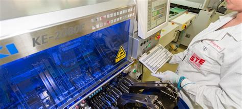
Once the solder paste is applied, the SMD components are placed onto the PCB pads. This process is typically automated using Pick-and-Place machines, which use vacuum nozzles to pick up components from feeders and place them accurately on the PCB. For prototyping or small-scale production, manual placement using tweezers can be employed.
Step 3: Reflow Soldering
After component placement, the PCB undergoes reflow soldering. The board is passed through a reflow oven, which heats the solder paste to its melting point, typically following a specific temperature profile. The molten solder then solidifies, creating a permanent electrical and mechanical connection between the component leads and the PCB pads.
Step 4: Inspection and Rework
After reflow soldering, the assembLED PCB is inspected for defects such as bridging, tombstoning, or missing components. Inspection can be performed visually, using magnification, or with the help of Automated Optical Inspection (AOI) systems. If defects are found, rework is necessary, which involves removing the faulty component, cleaning the pads, and resoldering a new component.

Checking SMD Components
Before assembling SMD components, it is essential to check them for proper functionality and to ensure they meet the required specifications. Some common checks include:
- Visual inspection: Examine the component for any visible damage, such as cracks, bent leads, or missing terminals.
- Polarity verification: Ensure that polarized components, such as diodes, LEDs, and electrolytic capacitors, are oriented correctly.
- Resistance measurement: Use a multimeter to measure the resistance of resistors and verify that they are within the specified tolerance.
- Capacitance measurement: Check capacitors using a capacitance meter to ensure they have the correct capacitance value.
- Diode testing: Test diodes using a multimeter’s diode mode to verify proper forward and reverse bias characteristics.
Frequently Asked Questions (FAQ)
1. What is the difference between SMD and through-hole components?
SMD components are designed to be mounted directly onto the surface of a PCB, while through-hole components have leads that are inserted into holes drilled in the PCB and soldered on the opposite side. SMDs are smaller and allow for higher component density, while through-hole components are larger and easier to handle manually.
2. Can I solder SMD components using a regular soldering iron?
While it is possible to solder some larger SMD components using a fine-tipped soldering iron, it is not recommended for smaller components or high-volume production. Reflow soldering using a reflow oven or hot air soldering station is the preferred method for SMD assembly.
3. What is tombstoning in SMD assembly?
Tombstoning, also known as drawbridging, is a defect that occurs when one end of an SMD component lifts off the PCB pad during reflow soldering. This can be caused by uneven heating, improper solder paste application, or component misalignment. Tombstoning can be prevented by ensuring proper stencil design, solder paste viscosity, and component placement accuracy.
4. How do I rework SMD components?
To rework an SMD component, first apply flux to the component and surrounding pads. Then, use a hot air soldering station to heat the component evenly until the solder melts. Remove the component using tweezers, and clean the pads using solder wick or a desoldering pump. Apply fresh solder paste and place a new component, then reflow solder the new component in place.
5. What are the most common package sizes for SMD components?
Some of the most common SMD package sizes include:
| Package | Dimensions (mm) |
|---|---|
| 0402 | 1.0 x 0.5 |
| 0603 | 1.6 x 0.8 |
| 0805 | 2.0 x 1.25 |
| 1206 | 3.2 x 1.6 |
| SOIC | 3.9 x 4.9 |
| TSSOP | 4.4 x 3.0 |
| QFP | Various sizes |
| BGA | Various sizes |
Conclusion
SMD assembly and checking are critical processes in the production of modern electronic devices. By understanding the advantages of SMDs, the assembly process, and proper component checking techniques, you can ensure the quality and reliability of your electronic assemblies. Although SMD assembly requires specialized equipment and skills, it offers numerous benefits, including smaller device sizes, higher component density, and faster production times.


Leave a Reply