Understanding Automated Optical Inspection (AOI)
Definition and Purpose
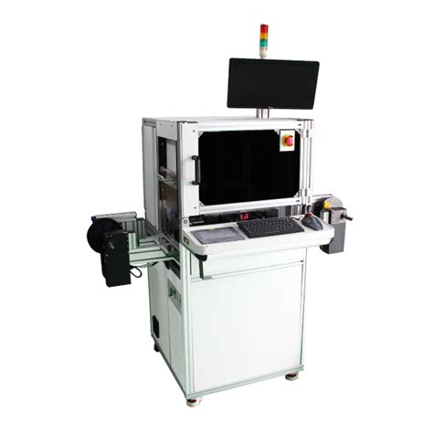
Automated Optical Inspection (AOI) is a non-contact, automated visual inspection method used to identify defects, errors, and inconsistencies in PCBs during various stages of the manufacturing process. The primary purpose of AOI is to catch defects early, reducing the need for costly rework and improving overall product quality.
How AOI Works
AOI systems utilize high-resolution cameras, advanced lighting systems, and powerful image processing software to capture and analyze images of PCBs. The captured images are compared against a “golden board” or a set of predefined rules to identify any deviations or anomalies. When a defect is detected, the AOI system alerts the operator, allowing for quick corrective action.
Benefits of Automated Optical Inspection
Increased Efficiency and Productivity
AOI systems can inspect PCBs at a much faster rate than manual inspection, significantly increasing production efficiency. This enables manufacturers to handle larger volumes without compromising on quality.
Improved Defect Detection and Reduction
AOI’s advanced imaging capabilities allow it to detect even the smallest defects that may be missed by the human eye. By catching defects early, manufacturers can reduce the number of defective products reaching customers, enhancing overall product quality and reliability.
Cost Savings and ROI
Implementing AOI in the manufacturing process can lead to significant cost savings. By identifying defects early, manufacturers can minimize the need for expensive rework and reduce scrap rates. Additionally, improved product quality translates to fewer warranty claims and returns, further reducing costs.
Consistent and Objective Inspection
Unlike manual inspection, which is subject to human error and inconsistency, AOI provides a consistent and objective inspection process. This ensures that all PCBs are held to the same quality standards, regardless of the operator or shift.

Types of AOI Systems
2D AOI Systems
2D AOI systems utilize top-down imaging to inspect the surface of PCBs. They are effective in detecting defects such as missing components, incorrect component placement, and solder bridging.
3D AOI Systems
3D AOI systems employ advanced imaging techniques, such as laser triangulation or structured light, to create a three-dimensional representation of the PCB. This allows for the detection of defects related to component height, coplanarity, and solder joint quality.
Inline vs. Offline AOI
Inline AOI systems are integrated directly into the production line, inspecting PCBs immediately after the assembly process. Offline AOI systems, on the other hand, are standalone units that inspect PCBs after they have been removed from the production line. Inline AOI offers real-time feedback and faster defect detection, while offline AOI allows for more thorough inspection and analysis.

Defects Detectable by AOI
AOI systems are capable of detecting a wide range of defects in PCBs, including:
| Defect Type | Description |
|---|---|
| Missing components | Components that are absent from their designated locations |
| Misaligned components | Components that are not properly aligned or centered |
| Incorrect component placement | Components placed in the wrong location or orientation |
| Solder bridging | Unwanted solder connections between pins or pads |
| Solder voids | Gaps or holes in solder joints |
| Insufficient Solder | Inadequate amount of solder on joints |
| Lifted leads | Component leads that are not properly soldered to the PCB pads |
| Damaged components | Components that are physically damaged or deformed |

Implementing AOI in PCB Manufacturing
Choosing the Right AOI System
When selecting an AOI system for a PCB manufacturing facility, several factors should be considered:
- Production volume and speed requirements
- Types of defects to be detected
- PCB complexity and component density
- Integration with existing manufacturing processes
- Budget and return on investment (ROI)
Integrating AOI into the Production Line
To maximize the benefits of AOI, it is essential to integrate the system seamlessly into the production line. This involves determining the optimal placement of the AOI machine, ensuring proper conveyor systems are in place, and establishing data Communication Protocols between the AOI system and other manufacturing equipment.
Training and Operator Skill
While AOI systems automate the inspection process, skilled operators are still required to set up, monitor, and maintain the equipment. Proper training should be provided to ensure that operators understand the capabilities and limitations of the AOI system, as well as how to interpret and act upon the defect data generated.
Continuous Improvement and Data Analysis
AOI systems generate valuable data that can be used to drive continuous improvement in the manufacturing process. By analyzing defect trends and patterns, manufacturers can identify root causes of recurring issues and implement corrective actions to prevent future occurrences. This data-driven approach helps to optimize the manufacturing process and further enhance product quality.
FAQ
-
Q: How does AOI differ from manual visual inspection?
A: AOI uses advanced imaging systems and computer algorithms to automatically inspect PCBs, while manual visual inspection relies on human operators to visually examine the boards. AOI is faster, more consistent, and can detect smaller defects that may be missed by the human eye. -
Q: Can AOI completely replace manual inspection?
A: While AOI is highly effective, it is not a complete replacement for manual inspection. Some defects, such as those related to component functionality or visual aesthetics, may still require human judgment. A combination of AOI and selective manual inspection often yields the best results. -
Q: How fast can AOI systems inspect PCBs?
A: The inspection speed of AOI systems varies depending on factors such as PCB complexity, defect types being detected, and the specific AOI technology used. However, AOI systems can typically inspect PCBs at a rate of several thousand components per minute, significantly faster than manual inspection. -
Q: Can AOI detect defects in both surface mount and through-hole components?
A: Yes, modern AOI systems are capable of detecting defects in both surface mount technology (SMT) and through-hole components. However, the specific defects detectable may vary depending on the AOI system’s capabilities and configuration. -
Q: How does AOI handle PCBs with different designs or configurations?
A: AOI systems can be programmed to inspect different PCB Designs or configurations. This is typically done by creating inspection programs or “recipes” specific to each PCB type. These programs define the inspection criteria, component locations, and acceptable tolerances for each board design. When a new PCB design is introduced, a new inspection program is created and loaded into the AOI system.
Conclusion
Automated Optical Inspection (AOI) plays a crucial role in ensuring the quality and reliability of printed circuit boards. By leveraging advanced imaging technologies and computer algorithms, AOI systems can quickly and accurately detect a wide range of defects, reducing the need for costly rework and improving overall product quality. As PCBs continue to increase in complexity and miniaturization, the importance of AOI in the manufacturing process will only continue to grow. By implementing AOI and continuously analyzing the data it generates, PCB Manufacturers can drive process improvements, reduce costs, and deliver high-quality products to their customers.


Leave a Reply