A schematic is a key part of the printed circuit board (PCB) design process. The schematic diagram visually represents the electrical connectivity and functionality of a circuit using standardized symbols and conventions. Developing the schematic is typically the first major step in creating a new PCB design.
In this article, we’ll explore schematic diagrams in depth – what they represent, how they are created, how to read them, the standards used, and how they relate to PCB layout. We’ll also look at the crucial role schematics play in enabling effective PCB development.
What does a schematic diagram represent?
A schematic provides an abstract visual model of the electrical circuits present on a PCB. It uses symbols and lines rather than realistic representations of each component. The schematic focuses on conveying the connections and relationships between parts rather than their physical details.
More specifically, the key elements represented within a schematic are:
- Components – Standardized symbols depict each electronic part in the design like integrated circuits (ICs), resistors, capacitors, transistors, connectors etc. These don’t reflect the actual physical package.
- Nets/Nodes – The lines connecting symbols represent electrical connectivity between components. When components are connected directly or indirectly, they are part of the same net or node. This shows how current flows through the circuit.
- Hierarchy – Multi-level schematics allow complex systems to be broken down into smaller interconnected sub-sheets and components. Hierarchy blocks show relationships between sections.
- Functions – Functional blocks, modules or “black boxes” illustrate the purpose of circuit sections at a high level, hiding underlying implementation details.
So in summary, the schematic provides a model of what components are present and how they are electrically connected together to implement required functions.
How is a schematic created?
Schematics are developed using computer-aided design (CAD) software tools like Altium, KiCad, OrCAD, Eagle, etc. These tools provide a graphical interface for the user to efficiently create and edit schematics. The process of creating a schematic involves these key steps:
1. Determine functional requirements
The target functions and specifications of the PCB design must be well defined upfront. These drive development of the schematic by determining what circuits and connectivity are required.
2. Research and select components
Choose parts like ICs, transistors, passives that provide the needed functionality and electrical characteristics for each section of the design.
3. Create component symbols
Add symbols to the CAD tool’s component library representing all the selected parts. Follow industry standard representations or create custom symbols.
4. Arrange and connect symbols
Drag, drop and wire up symbols on the schematic sheet to map out the logical connectivity between components needed to achieve the design functionality.
5. Annotate and document
Apply unique reference designators to each component symbol and add any useful notes on the sheet.
6. Validate circuit functionality
Use simulations or calculations to validate the circuitry provides the necessary performance before laying out the PCB.
With the schematic completed, the connectivity map is now defined and PCB layout can begin based on this “blueprint”.
How to read a schematic diagram
Being able to accurately interpret the symbols and connections on a schematic is a crucial engineering skill. Here are some tips on reading a schematic:
- Scan from left to right, top to bottom – This flow follows the logical flow of the circuit in most cases.
- Identify components – Associate each symbol on the schematic with the matching part on the bill of materials (BOM).
- Follow signal flow – Trace the connections between symbols to see how current flows through the circuit.
- Recognize hierarchies – Pay attention to any higher level blocks or multi-sheet references which indicate functional subgroups.
- Leverage annotations – Component designators and any text notes provide helpful insight into the purpose and layout of the schematic.
- Consider test/interface points – Look for test points, pads and ports that enable voltage measurements or interface connections.
- Check power distribution – Follow power rails and understand how components are connected to appropriate voltage sources.
- Analyze functionality – Consider the purpose of each section and how it logically relates to surrounding circuitry.
Developing a methodical approach to traversing the schematic diagram will help identify how key components interact to achieve the intended functions.
Industry standards used in schematics
To enable broad understanding and consistency, schematic diagrams follow accepted industry standards. Here are some of the most common standards applied:
IEEE Std 91/91a
A widely used set of guidelines for schematic symbols and conventions originally published by the IEEE in the 1970s. Covers many fundamental schematic elements.
IEEE Std 315
Expanded symbol standards from the IEEE Solid-State Circuits Society Committee focused on guidelines for integrated circuits.
IEC 60617
International Electrotechnical Commission standard for graphical symbols for schematics covering a very comprehensive set of electrical and electronic components.
ANSI Y32.2
American National Standards Institute guidelines for schematic documentation including symbols, conventions, sizes, line widths and fonts.
IEEE Std 1364
Defines the Verilog hardware description language (HDL) for describing electronic systems. Verilog can represent both schematics and be converted to PCB layout.
Adherence to standards ensures maximum clarity and portability for schematics. Designers should follow the guidelines as applicable when developing new schematic diagrams.
Relationship between schematics and PCB layout
The schematic serves as the basis for transforming an electrical circuit concept into the physical PCB layout. Here is how schematics relate to PCB layout:
- Schematic “nets” map directly to copper traces that physically link components on the PCB.
- Component symbols represent the parts that will be converted into footprints and 3D packages on the board.
- The logical connectivity in the schematic dictates the routing paths required on PCB layers.
- Interface points on the schematic correspond to physical interfaces on the board.
- Power rails in the schematic must be realized as conductors on inner PCB layers.
- Functional blocks in the schematic help define layout sections or zones.
So in essence, the schematic provides the electrical roadmap that the PCB layout implements in actual routed copper traces across layers. The PCB design software leverages the schematic connectivity model to plan physical routing and placement.
Why are schematics important in PCB design?
Schematics provide a range of benefits that make them a foundational and indispensable part of the PCB design process:
Visualization
Schematics allow engineers to conceptualize and “see” the circuit connectivity before creation of the physical board.
Communication
The schematic provides an efficient medium for collaborators to understand, discuss and evaluate a circuit design.
Simulation
Engineers can simulate circuit behavior based on the schematic to verify functionality before layout.
Documentation
Schematics document the high-level logic and connectivity of the PCB design for future reference.
Automation
PCB design tools automate many aspects of board layout and routing based on the schematic.
Debugging
Schematics assist debugging and testing by offering easy traceability of electrical connections.
For these reasons, developing the schematic is a pivotal first stage of the PCB design process.
Schematic design tips
Here are some helpful schematic design tips to create quality schematics and streamline PCB layout:
- Use hierarchy – Break up complex schematics into logical functional blocks or smaller sub-sheets to simplify layout.
- Get consensus on symbols – Collaborate with team members to align on schematic symbol conventions for consistency.
- Differentiate power nets – Use unique names or labels for different supply nets like VCC, VDD, etc.
- Plan test points – Include test pads connected to nets that require voltage monitoring or probing.
- Define connectors early – Add connector symbols and define interface nets to ease PCB layout.
- Mind your EM fields – Keep sensitive analog and digital sections separate to prevent noise coupling.
- Simulate first – Leverage simulation to verify circuit operation before finalizing the schematic.
- Use instruments wisely – Limit use of off-page instruments to simplify schematics. Bring key aspects on-page if helpful to layout.
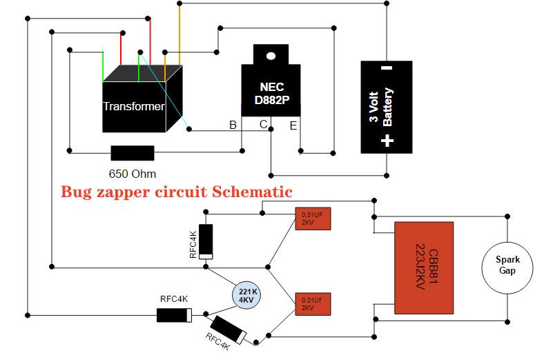
Sample schematic diagram analysis
Let’s look at an example schematic diagram to see the key concepts we’ve covered in practice. Here is a schematic for a simple electronic timer circuit:
Observing the schematic diagram reveals useful insights:
- The circuit uses a 555 timer IC as the central component, with supporting resistors and capacitors.
- Power connections are indicated, including 5V VCC supply rail.
- Inputs switch the circuit on or reset the timer period. LEDs visualize outputs.
- Standard IEEE symbols are used for the diode, capacitor, resistors, and IC.
- Reference designators and net names help identify components and connections.
- Notes provide key details on component values and the 555 timer configuration.
This level of analysis helps read and understand the circuit before layout begins.
Frequently asked questions about schematics
Here are answers to some common questions about schematic diagrams in PCB design:
Should schematics include component footprints and pin numbers?
Generally no – the schematic should focus on logical connectivity. Physical footprint details are better handled within the PCB design tool.
Do schematics require dimensionality or physical layout data?
Not typically. A schematic conveys logical, not physical relationships. Layout dimensions and constraints are usually managed separately.
Can schematics be auto-routed into a PCB layout?
Some simple designs can be automatically routed from schematics in tools like Fritzing. But for complex multi-layer boards, manual layout is still required.
What file formats are used to exchange schematics?
Common interchange formats are PDF, DXF, and modern tools use XML-based files. Older tools may also use netlist files or propriety formats.
Should testpoints be shown on schematics even if not used in production?
Yes, good practice is to include debug/test points needed during prototyping even if they are removed from the released product.
Conclusion
In summary, the schematic diagram is an essential element in PCB design, providing the visual circuit model that guides layout and enables engineering analysis. Adhering to standards like IEEE 91 helps maximize the clarity and portability of new schematic designs. With the schematic completed as the first major design step, the PCB layout process can then proceed efficiently, tracing out the required physical connectivity defined at the logical level. Combining schematic capture and PCB layout software helps streamline transforming an electrical concept through to fabricated boards successfully.


Leave a Reply