Introduction to PCB printing
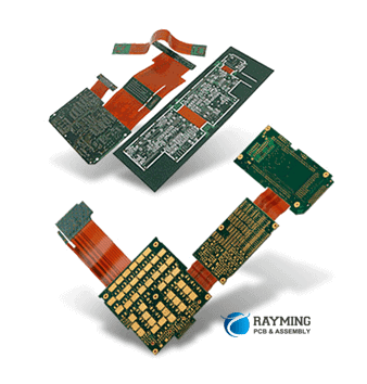
Printed circuit boards (PCBs) are essential components in modern electronics. They provide the base for mounting and connecting electronic components using conductive copper traces etched from copper sheets laminated onto a non-conductive substrate. PCB printing refers to the process of transferring the PCB design onto the copper-clad substrate to produce the conductive traces that form the electric circuits.
PCB printing enables rapid prototyping and iteration of electronic hardware designs. Instead of having PCB prototypes made by fabrication services that take days or weeks, you can print them yourself within hours. However, printing quality and capabilities are more limited compared to professional PCB fabrication. Home PCB printing is best suited for simple single-sided boards without extremely fine features.
This comprehensive guide will walk you through everything you need to know about printing your own PCBs. We’ll cover:
- PCB printing methods
- Required tools and materials
- PCB design considerations
- Step-by-step printing process
- Tips for troubleshooting and improving print quality
Equipped with this guide, you’ll have all the knowledge to start printing PCBs for your electronics projects at home. Let’s get started!
PCB Printing Methods
There are a few common methods to transfer a PCB layout onto the copper-clad substrate:
Laser/Inkjet Printer
A laser printer or inkjet printer can be used to print the PCB layout onto glossy magazine paper. An iron is then used to physically transfer the toner/ink layer from the paper onto the copper board through heat and pressure.
Advantages:
- Widely accessible and affordable
- Capable of very high resolution prints
Limitations:
- Inkjet ink does not always transfer well and requires special inkjet film
- Laser printed paper needs glossy, thicker magazine style paper
- Manual transfer with an iron is tedious and can cause distortions
UV Exposure
A UV exposure unit shines intense ultraviolet light through a printed transparency of the PCB layout onto a photosensitive copper board. The UV light causes chemical changes that allow the toner traces to remain while the rest of the photoresist coating washes away during development.
Advantages:
- Capable of high resolution transfers
- Automated exposure process ensures even transfers
Limitations:
- Requires transparency film printouts
- Photosensitive boards and chemical processing required
- UV exposure units can be expensive
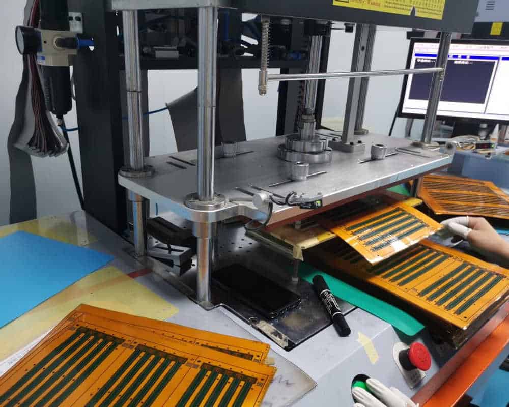
CNC Machining
A CNC machine uses a sharp bit to directly mill away the unwanted copper from a copper-clad board based on the PCB layout file.
Advantages:
- Does not require any special materials
- Can create complex multilayer boards
Limitations:
- Requires expensive CNC machine
- Lower resolution than printing methods
- Milling bits wear out over time
DIY Conductive Ink Pens
Special conductive ink pens can directly draw traces onto substrate boards to produce simple PCBs.
Advantages:
- Extremely simple and accessible
- Allows quick design iterations
Limitations:
- Very low durability and conductivity
- Only useful for very simple layouts
For home PCB printing, the laser/inkjet transfer method provides the best balance of accessibility, cost, and quality for simple boards. The exposure and CNC methods produce higher quality boards but require more expensive specialized equipment.
Required Tools and Materials
Here are the tools and materials you’ll need to print PCBs at home using the toner transfer method:
Tools
- Laser printer or inkjet printer
- Clothes iron
- Glass or metal plate bigger than PCB size
- scissors
- Drill for creating vias
- Safety gear – gloves, goggles, respirator mask
Materials
- Glossy magazine paper for laser printer toner transfer
- Inkjet PCB transfer paper if using inkjet printer
- Single or double-sided copper-clad substrate
- Etchant solution like ferric chloride for etching away copper
- Toner, acetone, or alcohol for cleaning boards pre and post transfer
- Rubbing alcohol and cotton balls for cleaning boards post-etch
- Optional: solder, flux, tin snips, soldering iron for preparing boards
The specific tools and materials required depends on the PCB printing method you choose. This list covers what’s needed for the toner transfer method, which provides the best balance of accessibility and print quality.
PCB Design Considerations
Your PCB layout must be designed with the capabilities and limitations of home PCB printing in mind. Here are some key considerations:
Trace Width and Spacing
The minimum trace width and spacing you can print is limited by the printer resolution. For a 600 DPI laser printer, traces and spaces under 8 mils may not transfer properly. Inkjet printers have lower resolution and require larger traces around 12 mils.
Alignment Viability
Alignment between both sides of a double-sided PCB can be difficult with home printing. Avoid having pads and traces spanning both sides of the board if possible.
Via Creation
Drilling holes for vias can be challenging without a drill press. Minimize vias, keep them large, or use foil punches. Routing traces to avoid vias is even better.
Number of Layers
Home PCB printing is only suitable for simple single or double-sided boards. Complex multilayer boards are not feasible. Keep layouts simple.
Component Selection
Use larger through-hole components when possible. Extremely tiny surface-mount components are difficult to hand solder at home without proper equipment.
Board Shape and Size
Standard rectangular boards are easier to clean, print, and etch consistently. Odd shaped boards can lead to issues with evenness of etching and transfer. Keep boards under 6 x 6 inches.
Following these PCB design considerations will ensure your layout is optimized for the home PCB printing process and avoid issues during transfer or etching.
Step-by-Step PCB Printing Process
Now let’s walk through the toner transfer PCB printing process step-by-step:
Step 1 – Design PCB Layout
Using PCB design software like KiCad or Eagle, design your printed circuit board layout adhering to the considerations mentioned earlier. Export the PCB layout as a high resolution image file.
Step 2 – Print Layout
Print the PCB layout image onto a glossy magazine paper using a laser printer if possible. For inkjet, use specialty inkjet PCB transfer paper. Print at the highest quality settings.
Step 3 – Clean and Prepare Copper Board
Cut the copper-clad substrate to size with scissors. Lightly scrub the board with toner, acetone, or alcohol using cotton balls to clean the copper surface and improve transfer.
Step 4 – Iron Transfer
Place the printed paper onto the copper board with the print side contacting the copper. Place a sheet of normal paper over this. Use the hot clothes iron (no steam) set to maximum heat to firmly iron over the paper for 2-3 minutes. The heat and pressure will soften the toner and transfer it onto the copper.
Step 5 – Etch Board
Peel away the paper after transfer is completed. Any areas with poor transfer can be manually touched up with a permanent marker. Submerge the board in ferric chloride etchant solution. Agitate periodically until all exposed copper is dissolved, leaving just the toner-protected traces.
Step 6 – Clean Board
Use rubbing alcohol and cotton balls to scrub away any toner or residue remaining on the PCB after etching. The result will be your design rendered in copper traces on the substrate.
Step 7 – Drill Holes
Use a power drill with small bits to manually drill holes for vias connecting both sides of the board if needed. Deburr holes afterwards.
Step 8 – Final Prep
Trim edges with tin snips, solder flux and pads if needed. The printed PCB is now ready to be populated with electronic components!
Troubleshooting Issues
Here are some common issues and solutions for troubleshooting home PCB printing:
Poor Toner Transfer
- Increase transfer time, pressure, and heat.
- Thoroughly clean copper before transfer.
- Try different paper types if using inkjet.
- Manually touch up any poor spots with marker before etching.
Scratches and Voids in Traces
- Avoid rough scrubbing when cleaning boards.
- Ensure boards stay completely still during etching.
- Increase toner thickness by printing 2-3 times.
Excess Undercutting During Etching
- Use fresh etchant solution.
- Reduce etching time and agitate more frequently.
- Ensure even consistent etching.
Misalignment Between Layers
- Minimize need for drilling holes with creative routing.
- Keep components only on one side if possible.
- Use mounting holes to line up both sides.
With practice, you will improve at avoiding and correcting these issues during the PCB printing process. Don’t get frustrated on your first attempts. Making lots of prototypes is the key to learning.
Improving Print Quality
Here are some tips for getting the highest quality PCB prints at home:
- Use a laser printer instead of inkjet. Toner transfers and adheres better.
- Print using the highest DPI settings and thickest paper to get the most toner on the paper.
- Get the smoothest, shiniest copper-clad laminates for easiest toner transfer.
- Maintain a hot even iron temperature and apply firm pressure for 3+ minutes when transferring.
- Agitate boards frequently in etchant and use a fan to circulate fumes away.
- Clean thoroughly between all stages using acetone/alcohol to remove residue.
- Go slow and be gentle when drilling to avoid cracks or scratches.
- Apply solder flux before soldering to all pads to prevent bridging.
Don’t expect professional quality right away. With refinement of your process and tools, your home printed PCBs can eventually look great.
FQA
What kind of substrates can I use for PCB printing?
The most common affordable PCB substrate is FR-4 fiberglass with copper laminated on one or both sides. This is the best type for home PCB printing. Other more advanced substrates like Rogers/Arlon PTFE composites are harder to print on.
Can I use a CNC machine to print PCBs at home?
Yes, you can use a desktop CNC mill or engraver machine to machine away copper directly instead of etching if you modify it with a carbide PCB milling bit. This eliminates the need for transfers and chemicals. The downside is lower resolution compared to photolithography techniques and the cost of a CNC machine.
What are the advantages of sending PCB designs to a professional fabrication shop vs home PCB printing?
Professional PCB fabrication offers much higher quality, smaller features, and complex multilayer boards with plated vias and soldermasks. However, turnaround times are slower and costs are higher. Home PCB printing trades off speed and quality for ultra-fast prototyping.
Should I use permanent marker or pen to touch up toner transfers?
Yes, permanent markers or etch-resist pens are great ways to manually fix spots with poor toner transfer before etching your board. Just ensure the marker/pen does not wash away in the etchant solution so it adequately protects the traces beneath it.
How many times can I reuse etchant solutions like ferric chloride for home PCB printing?
You can reuse etchant several times before it becomes saturated and loses effectiveness. Keep track of boards etched per volume and watch for slow etching times. Replace etchant once it no longer bubbles and etches quickly. Always add fresh etchant too to replenish solution. Proper storage extends lifetime.
Summary
I hope this guide has provided lots of useful advice on how to print your own PCBs at home using common tools and materials! With some practice, you’ll be able to churn out simple PCB prototypes with custom layouts in just a few hours rather than waiting days or weeks. This allows for much faster testing and iteration on your electronics projects. While home PCB printing has limitations compared to professional fabrication, the speed and accessibility benefits make it an invaluable tool for DIY prototyping.


Leave a Reply