1. Bridging
What is Bridging?
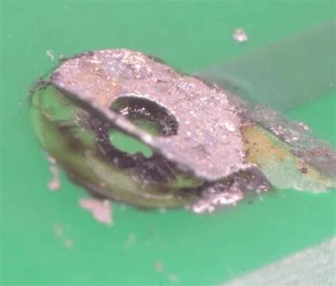
Bridging, also known as solder bridges, occurs when excess solder creates an unintended connection between two or more adjacent pads or traces on a PCB. This defect can lead to short circuits and cause the device to malfunction.
Causes of Bridging
- Excessive solder paste application
- Improper solder paste stencil design or alignment
- Incorrect reflow oven temperature profile
- Inadequate PCB cleaning prior to soldering
Solutions for Bridging
- Adjust solder paste application: Ensure that the solder paste is applied in the correct amount and location on the PCB pads.
- Optimize stencil design: Review and modify the solder paste stencil design to prevent excessive solder paste deposition.
- Fine-tune reflow oven settings: Adjust the reflow oven temperature profile to ensure proper solder melting and flow without causing bridging.
- Clean PCBs thoroughly: Implement strict cleaning procedures to remove any contaminants that may contribute to bridging.
2. Cold Solder Joints
What are Cold Solder Joints?
Cold solder joints occur when the solder fails to melt and flow properly, resulting in a weak, dull, and porous connection between the component lead and the PCB pad. These joints are often characterized by a rough or grainy appearance and can lead to intermittent or complete electrical failure.
Causes of Cold Solder Joints
- Insufficient heat during soldering
- Contaminated or oxidized component leads or PCB pads
- Improper flux application or activation
- Rapid cooling of the solder joint
Solutions for Cold Solder Joints
- Ensure adequate soldering temperature: Maintain the appropriate soldering iron temperature for the specific solder alloy and PCB material.
- Clean component leads and PCB pads: Remove any contamination or oxidation from the surfaces to be soldered using appropriate cleaning methods.
- Use high-quality flux: Select a suitable flux that promotes proper solder wetting and flow.
- Control cooling rate: Allow the solder joint to cool gradually to prevent the formation of cold joints.

3. Tombstoning
What is Tombstoning?
Tombstoning, also known as drawbridging, is a defect that occurs when a surface-mount component (SMD) stands up on one end, resembling a tombstone. This defect is typically caused by uneven heating or an imbalance in the solder paste volume on the component pads.
Causes of Tombstoning
- Uneven heating of the component during reflow
- Misaligned or uneven solder paste on the pads
- Incorrect component placement
- Differences in pad sizes or shapes
Solutions for Tombstoning
- Balance solder paste volume: Ensure that an equal amount of solder paste is applied to both pads of the component.
- Optimize reflow oven settings: Adjust the reflow oven temperature profile to provide even heating across the PCB.
- Verify component placement accuracy: Use automated placement machines or visual inspection to ensure proper component alignment.
- Equalize pad sizes and shapes: Design the PCB with equal pad sizes and shapes for each component to promote even solder melting and flow.

4. Solder Balling
What is Solder Balling?
Solder balling is a defect characterized by the formation of small, spherical balls of solder that are not properly connected to the PCB pads or component leads. These balls can cause short circuits and lead to device malfunction.
Causes of Solder Balling
- Excessive solder paste application
- Incorrect reflow oven temperature profile
- Contamination on the PCB or component surfaces
- Incompatible solder paste and surface finishes
Solutions for Solder Balling
- Optimize solder paste application: Control the amount and location of solder paste applied to the PCB pads.
- Adjust reflow oven settings: Fine-tune the reflow oven temperature profile to ensure proper solder melting and flow without causing balling.
- Maintain cleanliness: Keep the PCB and component surfaces free from contaminants that may contribute to solder balling.
- Select compatible materials: Choose solder paste and surface finishes that are compatible with each other to minimize the risk of solder balling.

5. Insufficient Solder
What is Insufficient Solder?
Insufficient solder, also known as a dry joint, occurs when there is not enough solder to create a strong, reliable connection between the component lead and the PCB pad. This defect can lead to weak or intermittent electrical connections and may cause the device to fail.
Causes of Insufficient Solder
- Inadequate solder paste application
- Incorrect solder paste stencil design or alignment
- Improper reflow oven temperature profile
- Oxidation or contamination of the component leads or PCB pads
Solutions for Insufficient Solder
- Increase solder paste application: Adjust the solder paste stencil design or application process to ensure an adequate amount of solder paste is deposited on the pads.
- Optimize stencil design: Review and modify the solder paste stencil design to ensure proper solder paste coverage on the pads.
- Fine-tune reflow oven settings: Adjust the reflow oven temperature profile to promote proper solder melting and flow.
- Clean surfaces thoroughly: Remove any oxidation or contamination from the component leads and PCB pads prior to soldering.
6. Solder Flags
What are Solder Flags?
Solder flags, also known as solder spikes or horns, are sharp, protruding bits of solder that extend from the solder joint. These defects can cause short circuits and may damage adjacent components or wiring.
Causes of Solder Flags
- Excessive solder paste application
- Incorrect reflow oven temperature profile
- Improper placement of components
- Contamination or oxidation of the soldering surfaces
Solutions for Solder Flags
- Control solder paste application: Ensure that the appropriate amount of solder paste is applied to the pads, avoiding excess.
- Optimize reflow oven settings: Adjust the reflow oven temperature profile to promote proper solder melting and flow without causing solder flags.
- Verify component placement: Use automated placement machines or visual inspection to ensure accurate component positioning.
- Maintain cleanliness: Keep the PCB and component surfaces free from contaminants and oxidation that may contribute to solder flag formation.
7. Lifted Pads
What are Lifted Pads?
Lifted pads occur when the copper pad on the PCB separates from the board substrate due to excessive heat or mechanical stress during the soldering process. This defect can lead to broken connections and device failure.
Causes of Lifted Pads
- Excessive soldering iron temperature
- Prolonged soldering time
- Insufficient PCB bonding strength
- Mechanical stress during component removal or rework
Solutions for Lifted Pads
- Control soldering temperature: Maintain the appropriate soldering iron temperature for the specific PCB material and component.
- Minimize soldering time: Limit the duration of heat application to the PCB pad to prevent lifting.
- Improve PCB bonding strength: Ensure that the PCB manufacturing process results in strong bonding between the copper pads and the board substrate.
- Use proper rework techniques: Follow recommended procedures for component removal and rework to minimize mechanical stress on the pads.
8. Solder Whiskers
What are Solder Whiskers?
Solder whiskers are thin, hair-like protrusions that grow from the surface of solder joints over time. These whiskers can cause short circuits and reliability issues in electronic devices.
Causes of Solder Whiskers
- Use of lead-free solder alloys
- Compressive stress in the solder joint
- Contamination or impurities in the solder
- Exposure to high temperatures or temperature cycling
Solutions for Solder Whiskers
- Select appropriate solder alloy: Choose solder alloys that are less prone to whisker formation, such as those containing lead or with specific additives.
- Minimize compressive stress: Design the PCB and components to reduce compressive stress in the solder joints.
- Ensure solder purity: Use high-quality solder with minimal impurities to reduce the risk of whisker growth.
- Control environmental conditions: Minimize exposure to high temperatures and temperature cycling, which can promote whisker formation.
9. Solder Voids
What are Solder Voids?
Solder voids are small, enclosed cavities within a solder joint that can weaken the connection and lead to reliability issues. These voids are typically caused by trapped gases or flux residue during the soldering process.
Causes of Solder Voids
- Improper flux activation or outgassing
- Incorrect reflow oven temperature profile
- Contamination or oxidation of the soldering surfaces
- Insufficient solder paste application
Solutions for Solder Voids
- Optimize flux selection: Choose a flux that is compatible with the solder paste and PCB surface finish, and ensures proper activation and outgassing.
- Adjust reflow oven settings: Fine-tune the reflow oven temperature profile to promote proper flux activation and minimize void formation.
- Maintain cleanliness: Keep the PCB and component surfaces free from contaminants and oxidation that may contribute to void formation.
- Ensure adequate solder paste application: Apply the appropriate amount of solder paste to the pads to reduce the risk of void formation.
Frequently Asked Questions (FAQ)
1. What are the most common PCB Soldering Defects?
The most common PCB soldering defects include bridging, cold solder joints, tombstoning, solder balling, insufficient solder, solder flags, lifted pads, solder whiskers, and solder voids.
2. How can I prevent bridging during PCB soldering?
To prevent bridging, ensure that the solder paste is applied in the correct amount and location on the PCB pads, optimize the stencil design, fine-tune the reflow oven temperature profile, and clean the PCBs thoroughly before soldering.
3. What causes cold solder joints, and how can I avoid them?
Cold solder joints are caused by insufficient heat during soldering, contaminated or oxidized component leads or PCB pads, improper flux application or activation, and rapid cooling of the solder joint. To avoid cold solder joints, ensure adequate soldering temperature, clean the surfaces to be soldered, use high-quality flux, and control the cooling rate.
4. How can I minimize the risk of tombstoning during PCB assembly?
To minimize the risk of tombstoning, balance the solder paste volume on the component pads, optimize the reflow oven settings for even heating, verify component placement accuracy, and equalize pad sizes and shapes on the PCB.
5. What steps can I take to reduce solder whisker formation?
To reduce solder whisker formation, select appropriate solder alloys that are less prone to whisker growth, minimize compressive stress in the solder joints, ensure solder purity, and control environmental conditions by minimizing exposure to high temperatures and temperature cycling.
| Defect | Causes | Solutions |
|---|---|---|
| Bridging | – Excessive solder paste application – Improper stencil design or alignment – Incorrect reflow oven temperature profile – Inadequate PCB cleaning |
1. Adjust solder paste application 2. Optimize stencil design 3. Fine-tune reflow oven settings 4. Clean PCBs thoroughly |
| Cold Solder Joints | – Insufficient heat during soldering – Contaminated or oxidized surfaces – Improper flux application or activation – Rapid cooling of the solder joint |
1. Ensure adequate soldering temperature 2. Clean component leads and PCB pads 3. Use high-quality flux 4. Control cooling rate |
| Tombstoning | – Uneven heating of the component – Misaligned or uneven solder paste – Incorrect component placement – Differences in pad sizes or shapes |
1. Balance solder paste volume 2. Optimize reflow oven settings 3. Verify component placement accuracy 4. Equalize pad sizes and shapes |
By understanding the causes and implementing the appropriate solutions for these common PCB soldering defects, manufacturers can significantly improve the quality and reliability of their electronic devices. Regular inspection, process control, and continuous improvement are essential for minimizing defects and ensuring the production of high-quality PCBs.


Leave a Reply