Introduction to PCB Stackup
Printed Circuit Board (PCB) stackup refers to the arrangement of copper and insulating layers that make up a PCB. The stackup design is crucial in determining the electrical properties, signal integrity, and overall performance of the PCB. In this article, we will delve into the world of 6 layer PCB manufacturing and explore the various stackup types available.
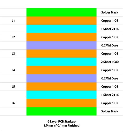
What is a 6 Layer PCB?
A 6 layer PCB is a printed circuit board that consists of six conductive copper layers separated by insulating layers. The increased number of layers allows for higher component density, improved signal integrity, and better power distribution compared to traditional 2 or 4 layer PCBs.
Advantages of 6 Layer PCBs
-
Increased Routing Density: With six layers available for routing, designers can accommodate more complex circuits and higher component counts within a smaller PCB area.
-
Improved Signal Integrity: The additional layers provide more options for signal routing, allowing for better control over impedance, crosstalk, and electromagnetic interference (EMI).
-
Enhanced Power Distribution: Dedicated power and ground planes in a 6 layer PCB ensure stable and clean power delivery to components, reducing noise and improving overall system performance.
-
Reduced Form Factor: By utilizing the extra layers, designers can miniaturize their designs and create more compact electronic devices.
6 Layer PCB Stackup Types
There are several stackup configurations commonly used in 6 layer PCB manufacturing. Each stackup type has its own characteristics and benefits. Let’s explore some of the most popular stackup types.
1. Signal-Signal-Ground-Power-Signal-Signal (SSGPSS)
The SSGPSS stackup is a widely used configuration in 6 layer PCBs. It consists of the following arrangement:
| Layer | Type |
|---|---|
| Top | Signal |
| 2 | Signal |
| 3 | Ground |
| 4 | Power |
| 5 | Signal |
| Bottom | Signal |
This stackup provides a good balance between signal integrity and power distribution. The ground and power planes in the middle layers act as reference planes for the signal layers, reducing crosstalk and providing a low-impedance return path for high-speed signals.
2. Signal-Ground-Signal-Power-Ground-Signal (SGSPGS)
The SGSPGS stackup is another common configuration for 6 layer PCBs. It offers improved signal integrity and EMI performance. The stackup arrangement is as follows:
| Layer | Type |
|---|---|
| Top | Signal |
| 2 | Ground |
| 3 | Signal |
| 4 | Power |
| 5 | Ground |
| Bottom | Signal |
In this stackup, the signal layers are shielded by ground planes on either side, reducing crosstalk and providing a stable reference for high-speed signals. The power plane is sandwiched between the two ground planes, ensuring a low-impedance power distribution network.
3. Signal-Signal-Power-Ground-Signal-Signal (SSPGSS)
The SSPGSS stackup is suitable for designs with a mix of analog and digital circuits. It provides separate power and ground planes for better isolation. The stackup arrangement is as follows:
| Layer | Type |
|---|---|
| Top | Signal |
| 2 | Signal |
| 3 | Power |
| 4 | Ground |
| 5 | Signal |
| Bottom | Signal |
This stackup allows for the separation of analog and digital power supplies, reducing noise coupling between the two domains. The central power and ground planes provide a low-impedance power distribution network and serve as reference planes for the signal layers.

Designing for 6 Layer PCB Stackup
When designing a 6 layer PCB, several factors need to be considered to ensure optimal performance and manufacturability. Here are some key guidelines:
-
Layer Assignment: Assign signals to appropriate layers based on their speed, sensitivity, and routing requirements. High-speed signals should be routed on the outer layers to minimize the dielectric thickness and reduce signal propagation delay.
-
Impedance Control: Use controlled impedance techniques to maintain signal integrity and minimize reflections. This involves selecting the appropriate trace width, spacing, and dielectric thickness based on the target impedance value.
-
Via Placement: Minimize the number of vias and place them strategically to reduce signal degradation and manufacturing complexity. Use blind and buried vias when necessary to optimize routing and reduce board size.
-
Power Distribution Network (PDN): Design a robust PDN by placing decoupling capacitors close to power pins, using wide and short traces for power distribution, and implementing proper power and ground plane geometries.
-
EMI Mitigation: Implement EMI mitigation techniques such as proper grounding, shielding, and filtering to reduce electromagnetic interference and ensure compliance with regulatory standards.

Choosing the Right 6 Layer PCB Manufacturer
Selecting a reliable and experienced 6 layer PCB manufacturer is crucial for the success of your project. Consider the following factors when choosing a manufacturer:
-
Manufacturing Capabilities: Ensure that the manufacturer has the necessary equipment, processes, and expertise to handle 6 layer PCB fabrication with the required specifications and tolerances.
-
Quality Control: Look for a manufacturer with strict quality control measures in place, including automated optical inspection (AOI), X-ray inspection, and electrical testing, to ensure the consistency and reliability of the manufactured PCBs.
-
Turnaround Time: Consider the manufacturer’s lead time and ability to meet your project timeline. Some manufacturers offer expedited services for time-critical projects.
-
Customer Support: Choose a manufacturer that provides excellent customer support, including technical assistance, design review, and prompt communication throughout the manufacturing process.

Frequently Asked Questions (FAQ)
-
What is the typical thickness of a 6 layer PCB?
A typical 6 layer PCB has a thickness of approximately 1.6mm to 2.0mm, depending on the dielectric material and copper weight used. -
Can 6 layer PCBs be manufactured with impedance control?
Yes, 6 layer PCBs can be manufactured with impedance control. The stackup design and material selection play a crucial role in achieving the desired impedance values. -
Are 6 layer PCBs suitable for high-frequency applications?
Yes, 6 layer PCBs are commonly used in high-frequency applications such as RF and microwave circuits. The additional layers provide better signal integrity and allow for the implementation of advanced routing techniques. -
What are the common materials used for 6 layer PCB fabrication?
Common materials used for 6 layer PCB fabrication include FR-4, Rogers, and Isola laminates. The choice of material depends on the electrical and thermal requirements of the application. -
How long does it typically take to manufacture a 6 layer PCB?
The manufacturing lead time for a 6 layer PCB varies depending on the complexity of the design, the chosen manufacturer, and the order quantity. Typical lead times range from 1 to 3 weeks, but expedited services may be available for faster turnaround.
Conclusion
6 layer PCBs offer numerous benefits, including increased routing density, improved signal integrity, and enhanced power distribution. Understanding the different stackup types and their characteristics is essential for designing high-performance electronic systems.
When designing a 6 layer PCB, careful consideration should be given to layer assignment, impedance control, via placement, power distribution network, and EMI mitigation techniques. Choosing a reputable and experienced PCB manufacturer is also crucial to ensure the quality and reliability of the manufactured boards.
By leveraging the advantages of 6 layer PCBs and following best design practices, engineers and designers can create compact, reliable, and high-performance electronic devices that meet the ever-increasing demands of modern applications.


Leave a Reply