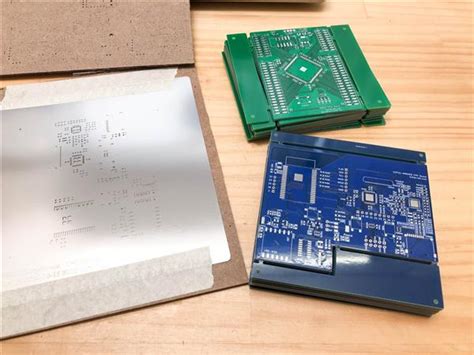
What Are PCB Stencil Openings and Why Are They Important?
PCB stencil openings are the areas on a printed circuit board (PCB) stencil where solder paste is deposited onto the PCB pads during the Solder paste printing process in PCB Assembly. The openings allow a precise amount of solder paste to be applied to create reliable solder joints between components and the PCB.
Properly designed PCB stencil openings are critical for several reasons:
-
Solder joint reliability – The right amount of solder paste deposited through well-designed stencil openings helps ensure strong, reliable solder joints. Too little solder paste can lead to open or weak joints, while too much solder paste can cause bridging or tombstoning defects.
-
Manufacturing efficiency – Consistent, high-quality solder paste printing enabled by optimal stencil openings reduces defects and rework, improving overall PCB assembly efficiency and throughput.
-
Miniaturization – As electronic devices shrink in size, PCBs are becoming more densely populated with smaller components. Precisely controlled solder paste deposition through finely tuned stencil openings is essential for assembling these miniaturized PCB designs.
-
Cost savings – Preventing solder defects with proper stencil opening design helps minimize scrap, rework, and production delays, ultimately reducing PCB assembly costs.
Given the importance of PCB stencil openings, let’s dive into five key tips for creating optimal openings that will enhance your solder paste printing process and PCB assembly results.
Tip 1: Size Stencil Openings Based on PCB Pad Dimensions
How PCB Pad Size Affects Stencil Opening Design
The dimensions of the PCB pads that need to receive solder paste are the starting point for determining the size of the corresponding stencil openings. Generally, the stencil opening should be slightly larger than the PCB pad to allow for proper solder paste release and to accommodate any slight misalignment between the stencil and PCB during printing.
However, the exact size difference between the pad and stencil opening, known as the overprint, depends on various factors such as:
- Pad size and shape
- Solder paste type and particle size
- Stencil thickness
- PCB Surface Finish
- Reflow profile
A common rule of thumb is to set the stencil opening overprint at 1-2 mil (25-50 μm) per side for standard SMT pads. However, this may need to be adjusted based on the specific factors mentioned above and the results of printing tests.
Stencil Opening Size for Different Pad Types
Different types of PCB pads and packages may require unique stencil opening designs to achieve optimal solder paste deposition. Here are some general guidelines:
| Pad/Package Type | Typical Overprint (per side) |
|---|---|
| Standard SMT | 1-2 mil (25-50 μm) |
| Fine-pitch SMT | 0.5-1 mil (12-25 μm) |
| BGA | 0-0.5 mil (0-12 μm) |
| QFN | 0.5-1 mil (12-25 μm) for perimeter pads, 0-0.5 mil (0-12 μm) for thermal pad |
These are just starting points and may need to be fine-tuned based on specific design requirements, manufacturing capabilities, and testing results.
Using Solder Paste Coverage Ratio for Opening Sizing
Another approach to sizing PCB stencil openings is to use the solder paste coverage ratio, which is the ratio of the stencil opening area to the PCB pad area. This method takes into account the effects of stencil thickness and solder paste properties on the volume of solder paste deposited.
A typical solder paste coverage ratio ranges from 0.66 to 0.80, meaning the stencil opening area is 66% to 80% of the pad area. The exact ratio to use depends on factors such as:
- Stencil thickness (higher ratio for thicker stencils)
- Solder paste type (higher ratio for no-clean paste compared to water-soluble)
- Pad size (higher ratio for larger pads)
- PCB surface finish (higher ratio for more solderable finishes like ENIG)
To calculate the stencil opening dimensions using the solder paste coverage ratio:
- Determine the appropriate ratio based on your specific PCB design and assembly process factors.
- Calculate the pad area by multiplying its length and width.
- Multiply the pad area by the solder paste coverage ratio to get the stencil opening area.
- Calculate the stencil opening dimensions by taking the square root of the opening area and adding the result to the pad length and width.
Here’s an example calculation for a 50 mil x 100 mil pad using a 0.75 solder paste coverage ratio:
Pad area = 0.050 in × 0.100 in = 0.005 in²
Stencil opening area = 0.005 in² × 0.75 = 0.00375 in²
Stencil opening dimensions = √0.00375 in² = 0.0612 in = 61.2 mil
Stencil opening length = 100 mil + 61.2 mil = 161.2 mil
Stencil opening width = 50 mil + 61.2 mil = 111.2 mil
Remember to round the final dimensions to the nearest manufacturing-capable value, typically to the nearest 0.1 mil or 1 μm.

Tip 2: Optimize Stencil Opening Shape for Solder Paste Release
Factors Affecting Solder Paste Release from Stencil Openings
The shape of PCB stencil openings plays a crucial role in how easily and consistently the solder paste releases from the stencil onto the PCB pads during printing. Several factors influence solder paste release, including:
-
Stencil opening wall smoothness – Smooth walls allow solder paste to release more easily, while rough walls can cause paste to stick and lead to inconsistent deposits.
-
Stencil opening aspect ratio – The aspect ratio is the relationship between the opening width and stencil thickness. A higher aspect ratio (narrower opening relative to thickness) can make paste release more difficult.
-
Solder paste properties – The rheology (flow characteristics) and tackiness of the solder paste affect how easily it releases from the stencil.
-
Printing parameters – Factors such as print speed, pressure, and separation speed influence the forces acting on the solder paste during the printing process and, consequently, its release from the stencil.
Common Stencil Opening Shapes and Their Benefits
Several stencil opening shapes are commonly used in PCB assembly, each with its own advantages:
| Shape | Description | Benefits |
|---|---|---|
| Rectangle | Simple rectangular opening that matches the PCB pad shape | Easy to design and manufacture, works well for most standard components |
| Rounded Rectangle | Rectangular opening with rounded corners | Reduces stencil wear and tear, improves paste release in corners |
| Circle | Circular opening for round PCB pads | Maximizes paste release due to lack of corners, ideal for BGA and CSP components |
| Diamond | Square opening rotated 45° relative to the PCB pad | Improves paste release by minimizing stencil opening aspect ratio |
| Teardrop | Elongated opening with one rounded end | Combines benefits of rectangle and circle, useful for QFN and DFN thermal pads |
The choice of stencil opening shape depends on the specific Component Types, PCB pad designs, and manufacturing capabilities. In some cases, a combination of shapes may be used to optimize solder paste deposition across a PCB.
Aperture Design Enhancements for Improved Paste Release
In addition to basic shape choices, several aperture design enhancements can be used to improve solder paste release from PCB stencil openings:
-
Tapered walls – Creating stencil openings with walls that taper outward (wider at the bottom) can help reduce the effects of high aspect ratios and improve paste release.
-
Nano-coating – Applying a nano-scale coating, such as a fluoropolymer, to the stencil surface and aperture walls can reduce solder paste adhesion and enhance release.
-
Stepped openings – For thicker stencils or high aspect ratio openings, a stepped design with a smaller opening at the top and a larger opening at the bottom can improve paste release while maintaining adequate volume.
-
Laser-cut apertures – Using laser cutting instead of chemical etching to create stencil openings results in smoother walls and better paste release, particularly for fine-pitch components.
By carefully selecting and optimizing the shape of PCB stencil openings, you can enhance solder paste release, achieve more consistent solder paste deposits, and improve the overall quality of your PCB assembly process.

Tip 3: Consider Stencil Thickness for Optimal Solder Paste Volume
How Stencil Thickness Affects Solder Paste Volume
The thickness of a PCB stencil directly impacts the volume of solder paste deposited onto the PCB pads. A thicker stencil will deposit more paste, while a thinner stencil will deposit less. Choosing the right stencil thickness is crucial for achieving the optimal solder paste volume for your specific PCB design and components.
The solder paste volume deposited through a stencil opening can be calculated using this formula:
Paste Volume = Stencil Thickness × Aperture Area × Paste Transfer Efficiency
Where:
– Stencil Thickness is the thickness of the stencil, typically measured in mils or microns
– Aperture Area is the area of the stencil opening, calculated by multiplying its length and width
– Paste Transfer Efficiency is a factor that accounts for the amount of paste that actually releases from the stencil and transfers to the PCB pad, typically ranging from 0.80 to 0.90 (80-90%)
Standard Stencil Thicknesses and Their Applications
PCB stencils are available in a range of standard thicknesses to accommodate different component types, package sizes, and solder paste requirements. Common stencil thicknesses and their typical applications include:
| Thickness (mils) | Thickness (μm) | Applications |
|---|---|---|
| 3-4 | 75-100 | Ultra-fine pitch components, 01005 passives |
| 4-5 | 100-125 | Fine-pitch components, 0201 passives, CSPs |
| 5-6 | 125-150 | Standard SMT components, 0402-0805 passives, QFPs, SSOPs |
| 6-8 | 150-200 | Larger SMT components, 1206-2512 passives, connectors |
| 8-10 | 200-250 | Through-hole components, power devices, RF shields |
These are general guidelines, and the optimal stencil thickness for your PCB assembly project will depend on your specific design requirements, component mix, and solder paste properties.
Determining the Optimal Stencil Thickness for Your PCB Design
To select the best stencil thickness for your PCB, consider the following factors:
-
Component types and sizes – Use the table above as a starting point based on your most common component types and sizes.
-
Solder paste properties – Consult your solder paste manufacturer’s recommendations for optimal stencil thickness based on the paste’s particle size and rheology.
-
PCB surface finish – More solderable finishes like ENIG may require slightly less solder paste (and thus a thinner stencil) compared to less solderable finishes like OSP.
-
Manufacturing capabilities – Ensure your chosen stencil thickness is compatible with your stencil manufacturing and PCB assembly equipment capabilities.
-
Prototype testing – Perform prototype runs with different stencil thicknesses and evaluate the resulting solder paste deposits and solder joint quality to determine the optimal thickness for your production runs.
In some cases, you may need to use different stencil thicknesses for different parts of the PCB, such as a thinner stencil for fine-pitch components and a thicker stencil for larger components. This can be achieved using a step stencil or multi-level stencil design.

Tip 4: Use Stencil Opening Modifications for Challenging Components
Challenges with Solder Paste Deposition for Certain Component Types
Some component types and package styles present unique challenges for solder paste deposition due to their size, shape, or thermal requirements. These include:
-
Fine-pitch components – Components with very small pin pitches (0.4 mm or less) require precise solder paste deposition to avoid bridging or insufficient solder volume.
-
Leadless packages – QFNs, DFNs, and other leadless packages have thermal pads that require a larger volume of solder paste compared to the perimeter pads.
-
Bottom termination components – BGAs, CSPs, and flip-chips have solder balls or bumps on the underside of the package, making it difficult to print solder paste directly onto the PCB pads.
-
Tall or heavy components – Connectors, RF shields, and other tall or heavy components may require additional solder paste volume to support their weight and maintain solder joint integrity.
Stencil Opening Modifications for Improved Solder Paste Deposition
To address these challenges, several stencil opening modifications can be employed:
-
Home plates for fine-pitch components – Extending the stencil openings for the outer pins of a fine-pitch component into a home plate shape can help anchor the component and improve solder joint strength.
-
Window panes for thermal pads – Creating a window pane pattern of smaller openings within the larger thermal pad stencil opening can improve solder paste release and reduce voiding.
-
Stepped openings for leadless packages – Using a stepped stencil design with a thicker stencil for the thermal pad and a thinner stencil for the perimeter pads can provide the necessary solder paste volume for each area.
-
Over-printing for bottom termination components – Printing solder paste onto the PCB area surrounding the pads for a BGA or CSP can help ensure sufficient solder volume and a more reliable solder joint.
-
Increased aperture size for tall or heavy components – Enlarging the stencil openings for tall or heavy component pads can provide additional solder paste volume to support the component weight and improve joint strength.
Here are some examples of how these modifications can be applied:
| Component Type | Modification | Illustration |
|---|---|---|
| Fine-pitch QFP | Home plate extensions on outer pin openings | |
| QFN thermal pad | Window pane pattern in thermal pad opening | |
| BGA | Over-printing surrounding the pad area |
Keep in mind that these modifications may require adjustments to your stencil design parameters, such as aperture size and shape, and may impact the overall stencil thickness. Always perform prototype testing to validate the effectiveness of any stencil opening modifications for your specific PCB design and assembly process.
Collaboration with PCB Design and Assembly Teams
Implementing stencil opening modifications for challenging components requires close collaboration between the PCB design and assembly teams. Designers should communicate any special component requirements or solder paste deposition challenges to the assembly team early in the design process.
The assembly team can then provide guidance on the most appropriate stencil opening modifications based on their experience and the capabilities of their stencil manufacturing and solder paste printing equipment. They may also recommend changes to the PCB pad design or component placement to facilitate optimal solder paste deposition.
By working together and considering stencil opening modifications as part of the overall PCB design and assembly process, you can ensure the best possible solder paste deposition and solder joint quality for even the most challenging components.
Tip 5: Implement Stencil Design Best Practices for Optimal Results
Stencil Design Guidelines for Manufacturability and Performance
To ensure the best possible solder paste deposition and PCB assembly results, follow these stencil design guidelines:
-
Aperture Size – As a general rule, stencil openings should be 1-2 mils (25-50 μm) larger than the corresponding PCB pads to allow for proper solder paste release and accommodate any misalignment.
-
Aperture Shape – Use the simplest shape that provides the necessary solder paste volume and release characteristics. Rectangles and circles are the most common shapes, but consider diamonds, teardr


Leave a Reply