Introduction
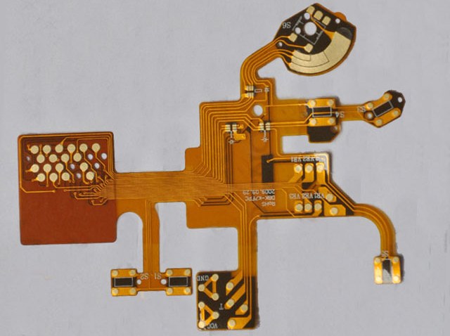
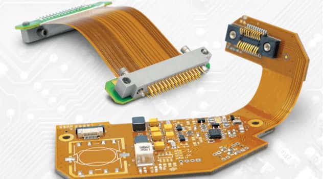
A flex PCB, also known as a flexible printed circuit board, is a type of PCB made of flexible materials that can bend and flex. Flex PCBs allow for more versatile PCB designs that can fit into tight or moving spaces.
4 layer flex PCBs contain 4 conductive copper layers separated by dielectric material. They provide more routing channels than 2 layer flex PCBs for complex circuit designs. 4 layer flex PCBs are commonly used in consumer electronics, medical devices, aerospace applications, and more.
In this article, we will explore what 4 layer flex PCBs are, their design considerations, manufacturing process, and applications.
What is a 4 Layer Flex PCB?
A 4 layer flex PCB contains 4 conductive copper layers that are laminated together with flexible dielectric insulation material in between. Here is an overview of the layer stackup:
| Layer Number | Layer Name | Description |
|---|---|---|
| 1 | Top / Signal | Outer layer used for component pads and routing |
| 2 | Ground | Ground plane for return paths |
| 3 | Power | Power plane for power distribution |
| 4 | Bottom / Signal | Outer layer used for component pads and routing |
The 4 conductive layers are sandwiched between 3 dielectric insulation flex core material layers. Common dielectric materials used are polyimide (PI) and polyethylene terephthalate (PET).
4 layer flex PCBs provide the following advantages compared to 2 layer flex PCBs:
- More routing channels – With 2 additional internal layers, complex routing is facilitated on a 4 layer flex PCB.
- Improved impedance control – The closely spaced ground and power planes allows for better impedance control for high speed signals.
- Lower EMI – The ground plane helps shield signals and reduce EMI emissions.
- Better power delivery – The power plane provides low impedance power distribution.
- Higher component density – Components can be placed on both sides.
4 Layer Flex PCB Design Considerations
Here are some important design considerations when working with 4 layer flex PCBs:
Flexibility – The bend radius should be considered early in the design to ensure the flex PCB can flex as needed without damaging the copper traces. Minimum bend radii range from 3-10x the board thickness depending on the materials.
Routing – Use wide traces and avoid acid traps. Follow IPC-2223 design guidelines. Build test coupons to dial in trace/space and analyze post-flexing.
Components – Use flex-friendly components rated for repeated bending. Avoid large, rigid components in flexing areas.
Stiffeners – Add stiffeners made of rigid material on non-flexing regions to prevent unwanted movement.
Adhesives – Use flex-grade adhesives suited for dynamic and repeated flexing.
Vias – Use capped or filled vias to avoid cracking. Avoid placing vias in high flexing areas.
Testing – Perform stress tests, thermal cycling, vibration, drop/shock testing to validate the design.
4 Layer Flex PCB Manufacturing Process
Here is an overview of the typical manufacturing process flow to fabricate a 4 layer flex PCB:
- Design – The PCB layout is designed with CAD software accounting for flex design rules.
- Film Processing – Layers of copper foil are laminated to dielectric core material. Photoresist is applied, exposed, and developed to form the desired copper pattern on each layer.
- Layer Alignment and Lamination – The 4 patterned circuit layers are precisely aligned and laminated together under heat and pressure. Registration accuracy is critical.
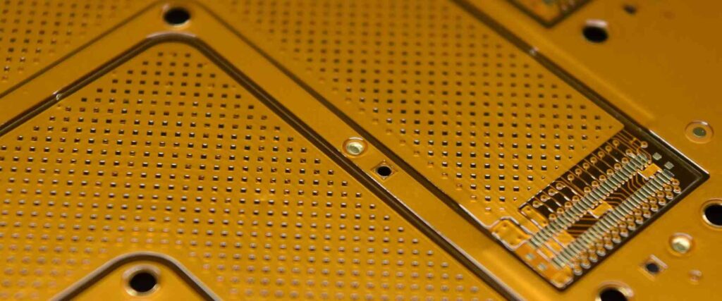
- Via Formation – Mechanical or laser drilling forms the holes for interlayer connections. The holes are then plated with copper.
- Solder Mask – Liquid photoimageable solder mask is applied over the surface, exposed, and cured. Openings are left for soldering.
- Legend Printing – Inkjet printing forms the legends and markings for component placement and polarity.
- Final Testing – Electrical testing validates connectivity. Optical inspection checks for defects.
- Singulation – The board outline is punched or routed to separate individual boards from the panel.
- Flex PCB Assembly – Components are soldered onto the flex PCB using SMT and/or through-hole assembly processes.
4 Layer Flex PCB Design Software
Here are some commonly used PCB design software tools for 4 layer flex PCBs:
- Altium Designer – Provides specialized flex and rigid-flex design features for trace widths, teardrops, bend compensation.
- Cadence Allegro – Offers a flex PCB design option with flex routing tools, dynamic bend radius checks.
- Mentor Xpedition – Integrated flex and rigid-flex design environment with autorouter aware of flex areas.
- Zuken CR-8000 – Has a flex rigid-flex board solution with modeling of physical stacks and traces over bends.
- Autodesk EAGLE – Low-cost tool with limited flex support but useful for simpler 4 layer flex PCBs.
Applications of 4 Layer Flex PCBs
Here are some common applications and products that utilize 4 layer flex PCB technology:
- Wearable devices – Activity trackers, smart watches, medical patches. A 4 layer flex allows routing in a thin, compact profile.
- Robotics – Arms, joints, and end effectors. Flex PCBs allow movement and reduce wires.
- Automotive – Around moving parts like folding rearview mirrors, rotatable displays, and hinged control panels.
- Consumer electronics – Cell phones, laptops, VR headsets. Flex PCBs connect mainboards to display panels.
- Medical – Ultrasound transducers, patient monitoring devices, implants. Conforms to body anatomy.
- Aerospace and defense – Satellites, rocketry, and avionics. Withstands vibration and thermal stresses.
As electronics become more compact and move into flexible form factors, demand for flex PCBs including 4 layer configurations continues to grow.
Frequently Asked Questions
Here are some common questions about 4 layer flex PCB technology:
Q: What are some typical dielectric materials used in 4 layer flex PCBs?
A: Common dielectric materials are polyimide (PI), polyethylene terephthalate (PET), polyethylene naphthalate (PEN). Polyimide provides the most flexibility.
Q: Does a 4 layer flex PCB need to be uniform thickness?
A: No, different sections can have different layer stackups. Some areas may just use 2 layers to maximize flexibility.
Q: Can components be mounted on both sides of a 4 layer flex PCB?
A: Yes, components can be placed on both outer layers during assembly. Vias connect traces on top and bottom layers.
Q: What are some challenges when designing a 4 layer flex PCB?
A: Key challenges are managing layer stackup, minimizing rigid sections, accounting for dynamic flexing, and adhesive selection.
Q: How small can the bend radius be for a 4 layer flex PCB?
A: The minimum bend radius depends on material selection but is typically 3-10 times the total board thickness.


Leave a Reply