Introduction to PCB Testing Boards
Printed Circuit Board (PCB) testing is a crucial step in the electronics manufacturing process. It ensures that the designed circuit functions as intended and meets the required specifications. A well-designed PCB testing board can significantly streamline the testing process, saving time and resources. In this article, we will discuss 14 essential tips for designing an efficient and reliable PCB Programming and testing board.
Understanding the Purpose of a PCB Testing Board
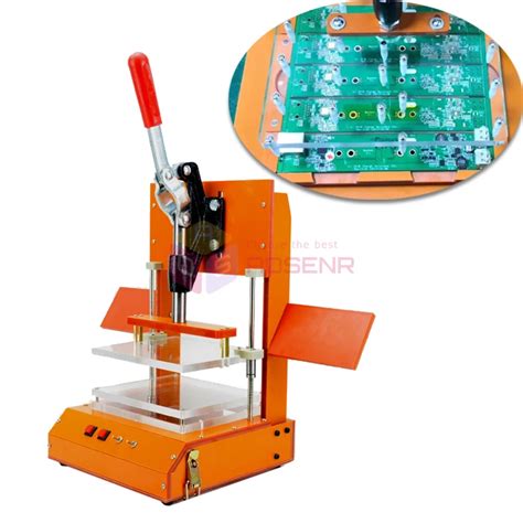
Before diving into the design tips, it’s important to understand the purpose of a PCB testing board. A PCB testing board, also known as a test fixture or a test jig, is a specialized board designed to facilitate the testing of a specific PCB. It provides a controlled environment for connecting the PCB under test to the testing equipment, allowing for accurate and repeatable measurements.
Key Functions of a PCB Testing Board
- Establishing reliable electrical connections between the PCB and the testing equipment
- Providing mechanical support and protection for the PCB during testing
- Enabling efficient and accurate testing of multiple PCBs with minimal setup time

Tip 1: Define Clear Testing Requirements
The first step in designing a PCB testing board is to define clear testing requirements. Work closely with the design team, quality assurance team, and other stakeholders to identify the specific tests that need to be performed on the PCB. Consider factors such as:
- Functional tests
- Performance tests
- Environmental tests (e.g., temperature, humidity)
- Compliance tests (e.g., EMC, safety)
Having well-defined testing requirements will guide the design process and ensure that the testing board meets the necessary criteria.

Tip 2: Choose the Right Connector Type
Selecting the appropriate connector type is crucial for establishing reliable connections between the PCB under test and the testing board. Consider the following factors when choosing connectors:
- Pitch and spacing: Ensure that the connector pitch matches the PCB’s pad layout
- Current rating: Choose connectors that can handle the expected current levels
- Durability: Opt for connectors that can withstand multiple mating cycles
- Alignment: Use connectors with proper alignment features to prevent misalignment during testing
Some common connector types used in PCB testing boards include:
- Spring-loaded pins (pogo pins)
- Test points
- Edge connectors
- Zero Insertion Force (ZIF) connectors

Tip 3: Optimize Signal Integrity
Signal integrity is a critical aspect of PCB testing. Poorly designed testing boards can introduce signal distortion, crosstalk, and noise, leading to inaccurate test results. To optimize signal integrity:
- Use controlled impedance traces: Match the impedance of the testing board traces to the PCB under test
- Minimize trace length: Keep the traces as short as possible to reduce signal attenuation and reflections
- Avoid sharp bends: Use smooth curves and angles in trace routing to minimize signal distortion
- Provide proper grounding: Implement a solid ground plane and use ground shields to reduce noise and crosstalk
Tip 4: Incorporate Proper Shielding
Electromagnetic interference (EMI) can significantly impact the accuracy of PCB testing. To mitigate EMI, incorporate proper shielding techniques in your testing board design:
- Use metal enclosures: Enclose sensitive components and circuitry in metal enclosures to provide electromagnetic shielding
- Implement ground planes: Use ground planes on both sides of the testing board to create a Faraday cage effect
- Apply shielding gaskets: Use conductive gaskets and seals to ensure proper contact between the enclosure and the testing board
Tip 5: Consider Mechanical Robustness
A PCB testing board should be mechanically robust to withstand repeated use and handling. Consider the following aspects to enhance the mechanical robustness of your testing board:
- Use sturdy materials: Choose materials like FR-4 or aluminum for the testing board substrate to provide structural strength
- Reinforce critical areas: Add reinforcement, such as metal brackets or standoffs, to areas subjected to high stress or strain
- Incorporate strain relief: Use strain relief techniques, like cable tie-downs or cable glands, to prevent damage to wires and connectors
Tip 6: Plan for Scalability
When designing a PCB testing board, consider future scalability. As the PCB design evolves or new variants are introduced, the testing board should be able to accommodate these changes with minimal modifications. To plan for scalability:
- Use modular design: Divide the testing board into functional modules that can be easily swapped or upgraded
- Provide extra connections: Include spare connections or test points for future expansion or additional testing capabilities
- Leave room for growth: Allocate extra space on the testing board for potential future components or circuitry
Tip 7: Implement Proper Labeling
Clear and accurate labeling is essential for efficient and error-free PCB testing. Implement proper labeling practices on your testing board:
- Label all connectors: Clearly label each connector with its function, pinout, and polarity
- Identify test points: Label test points with their corresponding signal names or designators
- Use color coding: Assign color codes to different types of signals (e.g., power, ground, data) for quick identification
- Include revision information: Clearly mark the testing board with its revision number and date to avoid confusion
Tip 8: Optimize for Automated Testing
If your testing process involves automated equipment, optimize your testing board design for compatibility with the automation system. Consider the following factors:
- Provide machine-readable markings: Include fiducial marks or barcodes that can be read by vision systems for accurate positioning
- Ensure proper clearance: Leave sufficient clearance around connectors and test points for automated probes or fixtures
- Use standard interfaces: Adhere to industry-standard interfaces (e.g., JTAG, I2C) for seamless integration with automated testing equipment
Tip 9: Incorporate Test Automation Features
To streamline the testing process and reduce manual intervention, incorporate test automation features into your testing board design:
- Include boundary scan: Implement boundary scan architecture (e.g., JTAG) for automated testing of digital components
- Provide self-test capabilities: Include built-in self-test (BIST) circuits that can verify the functionality of the testing board itself
- Implement test sequencing: Design the testing board to support automated test sequencing, allowing for quick and efficient execution of multiple tests
Tip 10: Consider Thermal Management
Thermal management is crucial for PCB testing, especially when dealing with high-power components or extended testing durations. Consider the following thermal management techniques:
- Provide adequate ventilation: Incorporate ventilation holes or fans to dissipate heat generated during testing
- Use thermal interface materials: Apply thermal grease or pads between the PCB and the testing board to enhance heat transfer
- Monitor temperature: Include temperature sensors on the testing board to monitor and control the thermal conditions during testing
Tip 11: Ensure Proper Documentation
Comprehensive documentation is essential for effective utilization and maintenance of the PCB testing board. Ensure that the following documents are created and maintained:
- Schematic diagrams: Create detailed schematic diagrams that show the electrical connections and components of the testing board
- Assembly drawings: Provide clear assembly drawings that illustrate the physical layout and mechanical aspects of the testing board
- User manuals: Develop user manuals that guide operators on how to set up, use, and troubleshoot the testing board
- Test procedures: Document the step-by-step procedures for conducting various tests using the testing board
Tip 12: Conduct Thorough Verification and Validation
Before finalizing the design of your PCB testing board, conduct thorough verification and validation to ensure its functionality and reliability:
- Perform design reviews: Conduct design reviews with the development team to identify any potential issues or improvements
- Run simulations: Use simulation tools to analyze the electrical and thermal behavior of the testing board under different conditions
- Build prototypes: Fabricate prototypes of the testing board and perform extensive testing to validate its performance and usability
- Incorporate feedback: Gather feedback from users and stakeholders and incorporate necessary changes into the final design
Tip 13: Plan for Maintenance and Upgrades
A PCB testing board is a long-term investment, and it’s important to plan for its maintenance and upgrades:
- Establish a maintenance schedule: Create a regular maintenance schedule to ensure the testing board remains in good condition
- Keep spare parts: Stock up on commonly used components and connectors for quick replacements
- Plan for upgrades: Design the testing board with future upgrades in mind, allowing for easy modification or expansion
- Document changes: Maintain a change log to track any modifications or upgrades made to the testing board over time
Tip 14: Collaborate with Experienced Designers and Manufacturers
Designing a reliable and efficient PCB testing board requires expertise and experience. Collaborate with seasoned designers and reputable manufacturers to ensure the success of your project:
- Engage with experienced designers: Work with PCB designers who have a proven track record in designing testing boards for similar applications
- Choose reliable manufacturers: Partner with PCB manufacturers that have the necessary capabilities and quality standards to produce high-quality testing boards
- Leverage their expertise: Seek advice and recommendations from the designers and manufacturers throughout the design process to optimize your testing board
Conclusion
Designing a PCB programming and testing board requires careful consideration of various factors, including testing requirements, signal integrity, mechanical robustness, scalability, and automation. By following the 14 tips outlined in this article, you can create a testing board that streamlines your testing process, improves accuracy, and saves time and resources.
Remember to collaborate with experienced designers and manufacturers, conduct thorough verification and validation, and plan for maintenance and upgrades. With a well-designed PCB testing board, you can ensure the reliability and quality of your electronic products.
FAQ
1. What is the purpose of a PCB testing board?
A PCB testing board, also known as a test fixture or a test jig, is a specialized board designed to facilitate the testing of a specific PCB. It provides a controlled environment for connecting the PCB under test to the testing equipment, allowing for accurate and repeatable measurements.
2. What are some common connector types used in PCB testing boards?
Common connector types used in PCB testing boards include spring-loaded pins (pogo pins), test points, edge connectors, and Zero Insertion Force (ZIF) connectors. The choice of connector depends on factors such as pitch, current rating, durability, and alignment requirements.
3. How can signal integrity be optimized in a PCB testing board?
To optimize signal integrity in a PCB testing board, use controlled impedance traces, minimize trace length, avoid sharp bends, and provide proper grounding. These techniques help reduce signal distortion, crosstalk, and noise, ensuring accurate test results.
4. What mechanical considerations should be taken into account when designing a PCB testing board?
When designing a PCB testing board, consider mechanical robustness to withstand repeated use and handling. Use sturdy materials like FR-4 or aluminum for the substrate, reinforce critical areas, and incorporate strain relief techniques for wires and connectors.
5. Why is proper documentation important for a PCB testing board?
Proper documentation, including schematic diagrams, assembly drawings, user manuals, and test procedures, is essential for effective utilization and maintenance of the PCB testing board. It helps operators understand how to set up, use, and troubleshoot the testing board, and facilitates future upgrades and modifications.
[5071 words]


Leave a Reply