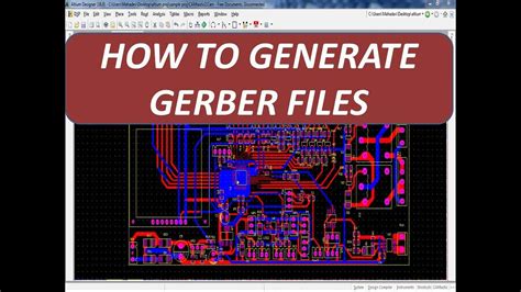
What is a Gerber File and Why is it Important?
A Gerber file, named after the company that created the format, is a standard file format used in the manufacturing of printed circuit boards (PCBs). It contains all the necessary information for a PCB manufacturer to fabricate the board, including the copper layers, solder mask, silkscreen, and drill data.
Gerber files are crucial in the PCB design process because they serve as the bridge between the design phase and the manufacturing phase. The accuracy and completeness of the Gerber files directly impact the quality and functionality of the final product.
9 Key Considerations for Gerber File Output
When outputting Gerber files for PCB manufacturing, there are several important factors to keep in mind to ensure a smooth and successful production process. Let’s discuss nine key considerations:
1. File Format Compatibility
Ensure that your Gerber files are in a format that is compatible with the manufacturer’s equipment and software. The most common formats are:
- RS-274X (Extended Gerber)
- ODB++ (Open Database++)
- IPC-2581 (GenCAM)
It’s essential to communicate with your manufacturer to determine their preferred file format and any specific requirements they may have.
2. Layer Naming Conventions
Use clear and consistent naming conventions for each layer in your Gerber files. This helps the manufacturer identify the purpose of each layer and reduces the risk of errors during production. A typical layer naming convention might include:
| Layer Name | Description |
|---|---|
| GTL | Top Copper |
| GBL | Bottom Copper |
| GTO | Top Overlay (Silkscreen) |
| GBO | Bottom Overlay (Silkscreen) |
| GTS | Top Solder Mask |
| GBS | Bottom Solder Mask |
| GTP | Top Paste Mask |
| GBP | Bottom Paste Mask |
| TXT | Drill File |
3. Aperture List
Include an aperture list with your Gerber files. An aperture list defines the shapes and sizes of the pads, traces, and other features on the PCB. This information is essential for the manufacturer to create the appropriate tooling for fabrication.
4. Drill File
Provide a separate drill file that contains information about the location, size, and type of holes required on the PCB. The drill file should include:
- Hole sizes
- Hole locations
- Plated or non-plated status
5. Solder Mask and Silkscreen
Ensure that your solder mask and silkscreen layers are properly defined in the Gerber files. The solder mask layer protects the copper traces from accidental shorts and corrosion, while the silkscreen layer provides text and symbols for component placement and identification.
6. Minimum Feature Size
Check that your design adheres to the manufacturer’s minimum feature size requirements. This includes:
- Minimum trace width
- Minimum gap between traces
- Minimum hole size
- Minimum annular ring
Failing to meet these requirements can result in manufacturing issues or reduced board reliability.
7. Panelization
If your design requires panelization (combining multiple PCBs into a single panel for production efficiency), include the necessary panel information in your Gerber files. This may include:
- Panel dimensions
- Tooling holes
- Fiducial marks
- Breakaway tabs
Consult with your manufacturer for their specific panelization requirements.
8. Overhang Mask
If you are designing PCBs that include selective gold plating, you need to include an overhang mask in your Gerber files. This layer specifies which areas of the board require gold plating and ensures that the plating process is accurate.
9. Gerber File Verification
Before sending your Gerber files to the manufacturer, verify that they are complete, accurate, and free of errors. Use a Gerber viewer to visually inspect each layer and check for any discrepancies or missing information. Many PCB design software packages include built-in Gerber viewers and design rule checks (DRC) to help identify potential issues.

FAQ
1. What happens if I don’t follow the manufacturer’s minimum feature size requirements?
If you don’t adhere to the manufacturer’s minimum feature size requirements, you may encounter issues during the fabrication process, such as:
- Traces or gaps that are too thin to be properly etched
- Holes that are too small to be drilled accurately
- Insufficient annular rings, leading to poor connection between layers
These issues can result in reduced board reliability, increased manufacturing costs, or even complete failure of the PCB.
2. Can I use different file formats for different layers in my Gerber files?
While it is technically possible to use different file formats for different layers, it is generally not recommended. Using a consistent file format throughout your Gerber files helps ensure compatibility with the manufacturer’s equipment and software, reducing the risk of errors and delays in the production process.
3. What is the difference between plated and non-plated holes in a drill file?
Plated holes are those that have a conductive metal coating on their inner walls, allowing electrical connection between layers of the PCB. Non-plated holes, also known as mechanical holes, do not have this conductive coating and are used for mounting components or other mechanical purposes.
4. How can I ensure that my solder mask and silkscreen layers are properly defined?
To ensure that your solder mask and silkscreen layers are properly defined, follow these guidelines:
- Use a clear naming convention for the layers (e.g., GTS for top solder mask, GBO for bottom silkscreen)
- Ensure that the layers are correctly aligned with the copper layers
- Adhere to the manufacturer’s minimum feature size requirements for solder mask openings and silkscreen line width
- Verify the layers using a Gerber viewer or design rule check (DRC) tool
5. What are the benefits of panelization in PCB manufacturing?
Panelization offers several benefits in PCB manufacturing, including:
- Increased production efficiency by allowing multiple PCBs to be fabricated simultaneously
- Reduced handling and testing time, as the panels can be processed as a single unit
- Improved board-to-board consistency, as all PCBs on a panel are exposed to the same manufacturing conditions
- Potential cost savings due to reduced setup time and material waste
However, panelization also requires additional design considerations, such as the placement of tooling holes, fiducial marks, and breakaway tabs. It’s essential to consult with your manufacturer to determine if panelization is appropriate for your specific project and to ensure that your design meets their requirements.

Conclusion
Outputting Gerber files for PCB manufacturing requires careful attention to detail and adherence to industry standards and manufacturer requirements. By considering the nine key factors outlined in this article – file format compatibility, layer naming conventions, aperture list, drill file, solder mask and silkscreen, minimum feature size, panelization, overhang mask, and Gerber file verification – you can ensure that your Gerber files are complete, accurate, and ready for a smooth manufacturing process.
Remember to communicate with your PCB manufacturer throughout the design and fabrication process to clarify any questions, address potential issues, and ensure that your final product meets your expectations.


Leave a Reply