Introduction
Printed circuit boards (PCBs) are essential components in most electronic devices. They provide mechanical support and electrical connections between electronic components using conductive tracks engraved from copper sheets laminated onto a non-conductive substrate.
Traditional PCBs use rigid insulating substrates like FR-4 (glass reinforced epoxy). But flexible PCBs use flexible insulating substrates like polyimide or transparent conductive polyester. This gives them distinct advantages in certain applications requiring dynamic flexing or conforming to curvilinear surfaces.
This article will compare flexible PCBs to traditional PCBs – their composition, manufacturing process, applications, pros and cons. A simple comparison table is also included summarizing the key differences.
Composition
Traditional PCB
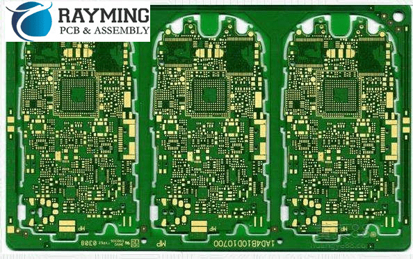
Traditional PCBs use FR-4 glass epoxy as the insulating substrate. It provides mechanical rigidity and dimensional stability needed for most electrical assemblies.
The substrate is clad with thin copper foil on one or both sides. The foil is etched using photolithography to produce required conductive tracks or pads.
Components are assembled by soldering their leads or terminals onto the pads. Hole plating or surface finishes like immersion silver, organic solderability preservative (OSP) etc. are applied to facilitate soldering.
Flexible PCB
Flexible PCBs replace the rigid FR-4 substrate with a thin flexible insulating material like polyimide (aka Kapton). This allows flexing, rolling, or bending of the PCB itself.
Polyimide sheets as thin as 12.5 microns (0.5 mil) are used to manufacture flexible circuits. Other flexible insulating materials like transparent PET, polyester, polyethylene etc. are also options.
Flexible substrates cannot withstand high temperatures. So lead-free soldering processes used for rigid PCBs are unsuitable. Conductive epoxy adhesives are commonly used to mount components onto flexible PCBs.
Manufacturing Process
Traditional PCB Fabrication
PCB fabrication involves multiple steps – substrate preparation, imaging, etching, plating, etc. Here are the key steps:
- Substrate preparation – Sheets of FR-4 are drilled and cleaned.
- Imaging – Photoresist is applied, exposed to UV, and developed to produce a mask.
- Etching – Unwanted copper is etched away, leaving behind desired tracks.
- Stripping and plating – Photoresist is stripped away. Surfaces are plated for solderability.
- Lamination – For multilayer PCBs, bonding sheets together under heat and pressure.
- Drilling – Holes are drilled for mounting components.
- Routing and scoring – Individual PCB outlines are cut away from panels.
- Testing and inspection – Ensuring quality requirements are met.
Sophisticated processes with automation produce affordable, high-quality PCBs in large volumes.
Flexible PCB Fabrication
Thin, fragile flexible substrates need special handling during fabrication. Polyimide sheets are bonded to rigid carrier frames to ease handling. Steps include:
- Bonding – Polyimide sheets are bonded to temporary carrier frames.
- Imaging – Similar to rigid PCB process. Done on both conductors and polyimide.
- Plating – Electroless Ni/Au plating provides solderability.
- Testing – Electrical testing and inspection.
- Debonding – Removal from carrier frame before further processing.
Photolithography and plating steps are adapted for the flexible material’s requirements. Components cannot be wave soldered. Routing and scoring require special custom tooling. Overall, flexible PCB fabrication needs greater process controls adding cost.
Applications
Rigid PCB Applications
Rigid PCBs dominate general purpose PCB applications like:
- Consumer electronics – TVs, DVD players, gaming consoles.
- Computers – Motherboards, interface cards, hobbyist projects.
- Home appliances – Ovens, smart thermostats, washing machines.
- Automotive electronics – Engine control units, infotainment systems.
Their mechanical rigidity provides easy assembly of components using automated SMT assembly and wave soldering. Multiple conductive layers interconnected by plated through holes support complex circuit routing in high density products.
Flexible PCB Applications
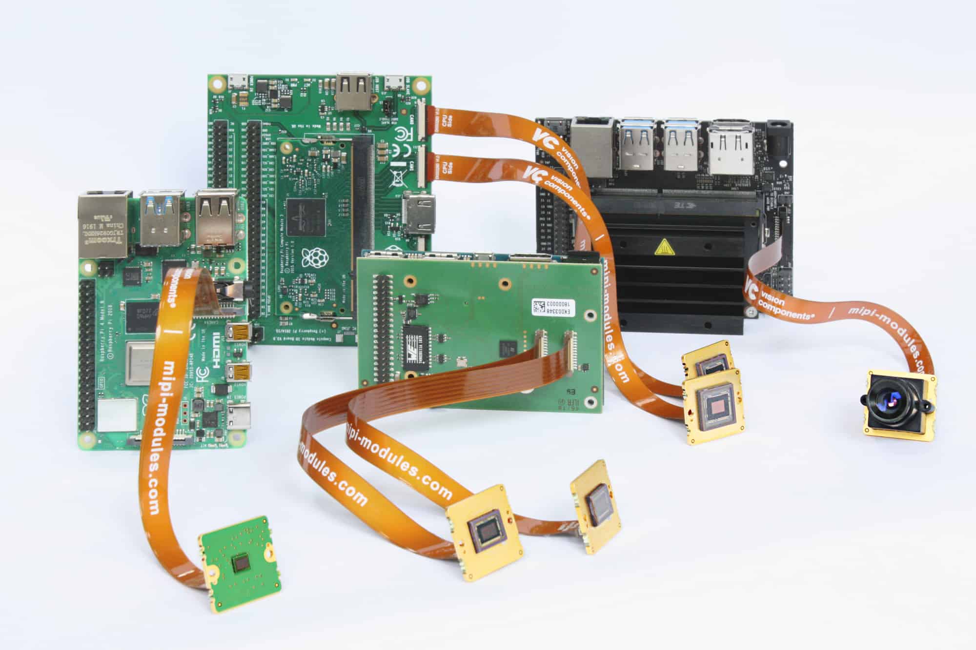
Flexible PCBs suit applications where dynamic flexing, bending or conforming to surfaces is required. For example:
- Wearable devices – Fitness bands, smart watches, VR headsets.
- Portable electronics – Cell phone flex cables, laptop flex connectors.
- Medical – Imaging sensors catheters that navigate arteries.
- Aerospace – Flex cables for instrument panels and controls.
- Sensors – Flex circuits with tactile, temperature, or strain gauges.
Flex circuits can dynamically adapt or wrap around surfaces. Built-in flexing withstands motion-induced fatigue better than wires or connectors. Thermal mismatch between silicon chips and substrates is also reduced.
Pros and Cons
Rigid PCBs
Pros
- Mechanically strong substrates for easy assembly and component mounting.
- Allows automated fabrication and assembly – lower costs.
- Allows high circuit complexity and density with multilayer boards.
- Can withstand harsh assembly environments – wave soldering, cleaning.
- Lowest cost option for mid to high volume products.
Cons
- Lack of flexibility limits applications involving flexing or conforming to contours.
- Susceptible to vibration and mechanical stresses.
Flexible PCBs
Pros
- Can dynamically flex and bend – suits applications with motion or odd shapes.
- Withstands vibration and mechanical stresses better.
- Lightweight and thinner than rigid options.
- Can be folded or rolled up for portability.
- Allows creative packaging, sculpture electronics, wearable devices.
Cons
- Component mounting and soldering is more difficult – costs are higher.
- Limited to 2-3 conductive layers – less suitable for complex circuitry.
- Flexibility varies with temperature – requires careful design.
- Polyimide substrates are more expensive than rigid FR-4.
Comparison Table
| Parameter | Rigid PCB | Flexible PCB |
|---|---|---|
| Substrate material | FR-4 glass epoxy | Polyimide, PET, Polyester |
| Thickness | 1.6mm, 2.4mm typical | 25 to 500 microns |
| Layers | Up to 20+ | 1-4 typical |
| Minimum track/gap | 150/150 μm (6/6 mil) | 125/125 μm (5/5 mil) |
| Component mounting | SMT, through-hole, connectors | Conductive adhesive, solder |
| Assembly process | Automated, low cost | Manual, high cost |
| Volume applications | Consumer electronics, computers | Wearables, sensors, medical |
| Withstands flexing | No | Yes |
| Cost | Lower | Higher |
FQA
What are some key differences between rigid and flexible PCBs?
Some key differences are:
- Rigid PCBs use stiff insulating substrates like FR-4 while flexible PCBs use thin insulating films like polyimide or PET.
- Rigid PCB manufacturing can be highly automated while flex PCB fabrication requires more manual steps.
- Flex circuits can dynamically bend and flex but rigid PCBs cannot.
- Rigid PCBs support more complex circuitry with higher layer counts while flex circuits are typically 1-4 layers.
- Component mounting methods differ – rigid PCBs use soldering while flex PCBs use conductive adhesive.
Why are flexible PCBs more expensive than rigid PCBs?
Flexible PCBs are more expensive due to several reasons:
- Raw materials like polyimide and adhesive films are more expensive than rigid FR-4.
- Flexible substrates require dedicated tools and careful handling during fabrication increasing costs.
- More process steps like debonding are manual or semi-automatic increasing labor costs.
- Lower volumes than consumer electronics mean lower economies of scale.
- Component assembly and soldering is typically manual which increases assembly costs.
- Testing/inspection requires special fixtures to simulate dynamic bending.
What are some key considerations when designing a flex PCB?
Some key design considerations for flex PCBs:
- Minimize rigid sections since flexing is concentrated on rigid-flex junctions.
- Plan fold areas carefully – ensure tracks can withstand expected bending cycles.
- Use tear-drop vias near junctions to improve flex life. Avoid plated through holes.
- Model stresses using FEA tools to predict flex circuit reliability.
- Specify minimum bend radius based on activities, materials used.
- Allow for thermal expansion, contraction effects during use.
- Place components in middle of flex areas instead of rigid sections.
What are some typical applications of flexible PCBs?
Some common applications are:
- Wearable devices – smart watches, fitness bands, health monitoring.
- Portable electronics – cellphone flex connectors, laptop flex cables.
- Medical – endoscopes, imaging sensors, hearing aids.
- Automotive – Flex circuits for steering wheel electronics, sensors.
- Industrial – Narrow flex circuits for motor windings and robot arms.
- Aerospace and military – Flex cables for avionics and displays.
What are some alternatives to using flexible PCBs for dynamic flex applications?
Some alternatives are:
- Rigid-flex PCBs – Integrates rigid and flexible substrates into one assembly.
- Cables or wire harnesses – Bundles of insulated wires assembled with connectors.
- Elastomeric connectors – Conductive rubber strips that can bend and compress.
- Spring contacts – Gold plated metal providing flexible contacts.
- Textile wiring – Conductive threads sewn into fabric, suitable for wearables.
- Metal mesh – Laser cut thin steel foil allowing flexing.
Each option has pros and cons and is suitable for certain use cases. Flex PCBs provide the most robust all-in-one interconnect solution for many applications.


Leave a Reply