Printed circuit boards (PCBs) are an essential component of most electronic devices. They provide the foundation on which components are mounted and connected. When designing a PCB, one important consideration is thickness. A thicker PCB will be more durable and better at dissipating heat. However, thicker PCBs also cost more to manufacture. For low-cost designs, finding the cheapest PCB thickness that still meets functional needs is important.
Factors That Affect PCB Thickness
There are several factors that influence the choice of PCB thickness:
Layer Count
The number of conductive copper layers in the PCB stackup impacts thickness. More layers allow for higher component density and complex routing, but increase cost and thickness. Single-sided boards are thinnest, followed by double-sided, and finally multilayer designs.
Copper Weight
Copper weight refers to the thickness of the copper foil used on the external layers of the PCB. Standard weights are 1 oz (35 μm) and 2 oz (70 μm). Heavier copper provides better current handling and heat dissipation. However, it also increases cost and thickness.
Dielectric Material
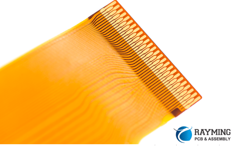
The insulating substrate that separates copper layers also influences thickness. Common rigid PCB dielectrics include FR-4 glass epoxy, polyimide, and PTFE. Flexible circuits use polyimide or polyester films. Thinner materials reduce weight and cost but sacrifice durability.
Board Size
Larger PCBs are prone to warping without sufficient thickness for mechanical rigidity. Small boards can use thinner profiles.
Component Height
Tall components require a thicker board to avoid exceeding the maximum height. Shorter components allow thinner PCBs.
Environmental Factors
PCBs in harsh environments may need thicker profiles for increased longevity and reliability. Thinner boards are acceptable for benign operating conditions.
Thermal Loads
High-power circuits generate significant heat. Thicker boards help transfer heat and avoid warping. Low-power digital circuits can use thinner, cheaper PCBs.
Frequency
At higher frequencies, transmission lines on PCBs begin to act as antennas, radiating signals. A thicker board with closer layer spacing helps control electromagnetic interference.
Standard PCB Thicknesses
PCB manufacturers offer a range of standard thicknesses to choose from. Here are some typical values starting from the thinnest:
0.4mm (0.016″)
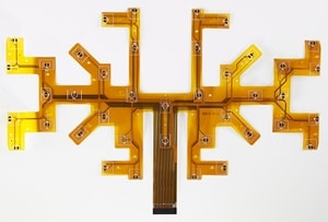
Extremely thin PCBs down to 0.4mm are usually single-sided or double-sided boards made from flexible dielectric films like polyimide. They are very low cost but have limited functionality. Applications include simple circuits like wearables, IoT devices, and flex/rigid-flex interconnects.
0.6mm (0.024″)
0.6mm provides some added robustness over 0.4mm and can optionally support 2-4 mil thick single-sided copper layers. Polyester and polyimide flex materials are common. Rigid glass epoxy FR-4 can potentially be used but is prone to warping. Best for simple interconnections and low layer count circuits without tall components.
0.8mm (0.031″)
0.8mm supports 4 mil copper layers while remaining compact. Polyimide and polyester flexible PCBs are options. Some FR-4 rigid boards are also viable at 0.8mm. Provides more versatility over thinner boards. Cost remains low.
1.0mm (0.039″)
At 1.0mm, cost increases but designs have fewer physical limitations. Polyimide flex materials as well as rigid FR-4 boards are commonly available. Supports 4-6 mil copper layers. Good for small rigid boards with low component height and layer count. Also useful for flexible circuits with dynamic bending requirements.
1.2mm (0.047″)
A common standard thickness for affordable 2-4 layer rigid FR-4 PCBs. 6 mil copper can be accommodated. Provides adequate physical strength for many rigid board designs. Flexible polyimide circuits can also leverage 1.2mm thickness. Overall a versatile and cost-effective option.
1.6mm (0.063″)
1.6mm is a widely used thickness for 4-6 layer rigid FR-4 boards. Supports 1oz/2oz copper and components up to 10mm tall. Provides robust mechanical properties with only a moderate cost increase versus thinner boards. A good compromise between cost, thickness, and performance.
2.0mm (0.079″)
2mm is common for 6-8 layer rigid boards using FR-4 dielectric. Also strong enough for large form factor boards over 200mm. Provides headroom for tall components, high layer counts, and good thermal/mechanical performance. Cost rises accordingly but overall an affordable standard for medium complexity PCBs.
2.4mm (0.094″)
At 2.4mm and above, PCBs support advanced functionality with high layer counts, thick copper weights, embedded passives/actives, and thermal challenges. Common for multilayer high density interconnects. Cost increases significantly but may be necessary for cutting-edge electronics.
Cheapest Viable Rigid PCB Thickness
For many cost-sensitive rigid PCB designs, 1.6mm provides the best tradeoff between capability and cost. It is a widely available standard thickness that supports the needs of common 4-6 layer boards with medium component heights and thermal loads. While 1.2mm or even 1.0mm can be cheaper, the more limited performance often necessitates higher layer counts or other compromises to achieve basic functionality. At only ~10% thicker than 1.2mm boards, 1.6mm delivers excellent value for money in terms of robustness and manufacturing yield.
Cheapest Viable Flexible PCB Thickness
For flexible PCBs, polyimide films around 0.1-0.2mm are often the cheapest functional option. Materials like polyester can potentially be thinner and cheaper but are far less durable with lower temperature tolerance. Polyimide below 0.2mm provides basic physical robustness and solder joint reliability while remaining compact and affordable. As a bonus, thin polyimide films inherently resist warping. For most cost-driven flexible circuit designs, 0.1mm is a good starting point with 0.2mm offering more headroom on thickness.
How Thickness Impacts PCB Cost
Why does increasing PCB thickness raise manufacturing costs? There are a few key factors:
- Material Costs: Thicker dielectric substrates require more raw material. Similarly, heavier copper foils use more metal.
- Waste and Processing: Thicker boards may require longer drilling, routing, and etching times. More material is consumed due to kerf loss from cutting. Reject rates can also increase.
- Layer Registration: Aligning and laminating more layers together with tight tolerances is challenging and may result in more scrapped boards.
- Panel Utilization: Panelization efficiency decreases as board thickness goes up. Panel sizes and thickness have limits which prevent fully dense packing of thick boards.
- Shipping Costs: Thicker and heavier PCB panels or assembled boards cost more to ship.
On a per unit area basis, PCB cost generally increases linearly with thickness. The incremental cost depends on the materials and manufacturing processes used. In practical terms, going from 1.6mm to 2.4mm could double the cost while a 0.4mm bump in thickness might add 5-10% cost.
When Thicker PCBs Are Worth It
While thinner PCBs are cheaper, sometimes extra thickness is needed to make a design feasible or hit performance targets.
Consider using thicker boards when:
- High layer counts (>8 layers) are required for routing density
- Multiple high speed signals need careful impedance control
- Large board dimensions (>250mm) require structural rigidity
- Tall components (>15mm) must be accommodated
- High power circuits demand improved thermal dissipation
- Sensitivity to vibration/flexing necessitates sturdiness
- RF signals and antennas benefit from thicker dielectrics
- Extra thickness reserves future design headroom
In these situations, the additional design flexibility and performance from thicker PCBs outweighs the cost premium.
How To Reduce PCB Thickness Costs
Some techniques to avoid unnecessary thickness and save money:
- Specify thickness only as thick as needed, not just default values
- Use thinner dielectric materials when flexibility allows
- Convert rigid sections to flex circuits to reduce area
- Look for free board space to place tall components horizontally
- Use smaller via sizes or laser microvias to save layers
- Select 0402 discretes over 0603 to allow thinner boards
- Consolidate components into ICs to enable thinner profiles
- Reduce copper weights if electrical current limits allow
- Try rigid-flex boards to optimize thick and thin areas
- Stack modules vertically to avoid large horizontal PCBs
- Use double-sided boards instead of multilayers when possible
- Route critical signals on outer layers for thinner dielectrics
Making informed design decisions about PCB thickness can lead to notable material and manufacturing cost savings.
Frequently Asked Questions
What is the typical PCB thickness for hobbyist projects?
For hobbyist PCBs made in small quantities, 1.6mm is a common standard thickness. It provides a good balance of cost, availability, and versatility for DIY electronics projects. 1.2mm can also be suitable when minimizing thickness and maximizing rigidity are not critical requirements.
How thick should a 2 layer PCB be?
For a simple 2 layer board, 1.2mm or 1.6mm are typical thicknesses. 1.6mm allows supporting taller components up to 10mm while 1.2mm provides a thinner, more cost effective choice for low-profile designs under 3-5mm height. 2 layer boards rarely need to exceed 1.6mm.
What PCB thickness is required for PCI/PCIe slots?
Most PCI and PCIe card edge connectors are designed for 2.4mm thick boards. This provides mechanical strength for large plug-in cards, allowing them to be securely inserted in slots without warping or damage. Thinner boards would flex excessively.
Can flex PCBs replace rigid PCBs to reduce thickness?
In many cases, thin polyimide flex PCBs under 0.2mm can replace rigid boards up to 1.6mm thick. Flex circuits intrinsically resist warping while providing interconnects and mounting pads for SMT components. Rigid sections can be laminated where structural strength is needed.
What is the typical PCB thickness used in cell phones?
Cell phone PCBs prioritize minimal thickness. Common dimensions are 0.4mm to 0.8mm using flexible polyimide or polyester substrates. Rigid FR-4 layers may be added in stacked regions requiring stiffness. Thicknesses up to 1.2mm are possible in folding phone hinge areas.


Leave a Reply