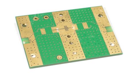
What is the PCB Bottom?
The PCB Bottom refers to the side of the printed circuit board opposite the component side (top side). It is the side that typically faces downward when the board is installed in a device. The bottom side contains the bulk of the copper traces that electrically connect the components on the top side.
Some key features and functions of the PCB Bottom include:
- Copper traces for routing signals between components
- Solder pads for surface mount components
- Vias (plated through holes) to connect traces on different layers
- Ground planes and power planes for shielding, current distribution, etc.
- Silkscreen labels and identifiers
- Test points for probing signals
- Exposed copper areas for heatsinking or shielding
So in summary, the PCB Bottom contains critical interconnects and features that enable the circuit to function, even though most components are mounted on the top side.
PCB Bottom Copper Layers
The conductive copper traces on the PCB Bottom are arranged in layers. Most PCBs will have at least one bottom copper layer, but complex designs can have multiple layers (4, 6, 8 or more) with traces and planes sandwiched in the middle of the board.
The copper weight or thickness on the bottom is typically 1 oz (35 μm) or 2 oz (70 μm). Thicker 2 oz copper is used for high current traces, while 1 oz is sufficient for signal routing.
The bottom layers are numbered in sequence, for example:
| Layer | Name |
|---|---|
| Top | Component side |
| 2 | Ground plane |
| 3 | Power plane |
| 4 | Bottom signal |
| Bottom | PCB Bottom |
The arrangement, thickness, and purpose of the bottom copper layers is defined in the PCB layer stackup drawing. Inner layers are laminated with insulating prepreg material.

PCB Bottom Assembly (SMT)
Many PCBs use surface mount technology (SMT) where components are soldered directly to pads on the surface of the board without through-holes. SMT components can be mounted on the top or bottom side of the PCB.
Bottom side SMT Assembly has some advantages:
- Allows for double-sided component mounting to save space
- Shorter trace lengths vs routing to the top side
- Enables the use of leadless packages (QFN, DFN, etc.)
However, there are also some challenges with bottom side SMT:
- Need selective solder mask and paste for bottom pads only
- Smaller components are harder to place and inspect
- Risk of tombstoning during reflow if not balanced
- May require special fixturing for wave soldering
For these reasons, the majority of SMT parts are often placed on the top side when possible. The PCB Bottom is used more for routing and interconnect.

PCB Bottom Silkscreen
The silkscreen is the white text and drawings printed on the PCB. The bottom silkscreen typically contains the following information:
- Board identifier (name, revision, serial number)
- Company logo and/or regulatory marks (CE, FCC, WEEE, etc.)
- Assembly drawing notes and instructions
- Component identifiers for bottom side parts
- Test point labels (TP1, TP2, GND, etc.)
- Pin 1 indicators and polarity marks
- PCB manufacturer markings
The bottom silkscreen helps with assembly, test, and field service of the PCB. Care must be taken that silk markings do not overlap solder pads.

PCB Bottom Solder Mask
Solder mask, also known as solder resist or solder stop, is the green (or other color) coating on the PCB that covers the copper traces but leaves the pads exposed. It prevents solder bridging and corrosion.
On the PCB Bottom, the solder mask openings must be precisely aligned to the SMT pads and vias. Misregistration can lead to open circuits or poor solder joints.
Selective areas of the solder mask may be left open on the bottom for purposes such as:
- Exposing large copper areas for heatsinking
- Defining SMT pads without solderpaste stenciling
- Edge connector contacts
- Castellated vias and holes
- Grounding contact points
- Test points
The PCB Bottom solder mask can also be a different color than the top for cosmetic reasons. The color has no effect on functionality.
PCB Bottom Ground Planes
A ground plane is a large area of copper on the PCB, typically on an inner layer, that is connected to the common 0V reference point. The PCB Bottom layer can also be a ground plane in some designs.
Ground planes serve several important functions:
- Provide a low-impedance return path for signals
- Reduce electromagnetic interference (EMI)
- Distribute heat evenly across the board
- Offer mechanical stability and rigidity
Connecting the ground pins of through-hole components to the bottom ground plane is done with vias. SMT components can also stitch their ground pads to an inner plane with micro-vias.
The PCB Bottom ground plane should have a copper keep-out area around the edge of the board to prevent shorts. Stitching vias are used to tie all the ground planes together at regular intervals.
PCB Bottom Design Guidelines
Here are some general guidelines to follow when designing the bottom of a PCB:
- Route signal traces on the bottom layer horizontally (side to side)
- Avoid routing traces under crystals, oscillators, connectors, or switches
- Provide adequate clearance around mounting holes and vias
- Do not place vias or traces under stress-sensitive components
- Minimize the use of vias in high-speed traces to avoid stubs
- Stitch ground planes together every 1/20 wavelength
- Flood unused areas with copper pour connected to ground
- Keep SMT pads and traces away from the edge of the board
Following these rules will help ensure good signal integrity and minimize manufactured defects and failures in the field.
Frequently Asked Questions (FAQ)
What is the BOTTOM layer of a PCB called?
The BOTTOM layer of a PCB is often called the “solder side” since through-hole component leads are soldered on the bottom. It may also simply be referred to as the PCB Bottom.
Which side of the PCB is the bottom?
The bottom of the PCB is the side opposite to where most of the components are mounted. It is the side that faces down when the board is installed in its enclosure or chassis.
How many copper layers are on the PCB bottom?
The number of copper layers on the PCB Bottom depends on the overall layer count. In a 2-layer board, the bottom is the only other copper layer besides the top. In multi-layer boards, the bottom is typically a signal routing layer but can also be a ground plane in some stackups.
Can SMT components be mounted on the PCB bottom?
Yes, SMT components can be mounted on the PCB Bottom side just like the top side. Double-sided SMT assembly is commonly used to save space. However, the majority of SMT parts are often placed on the top side for ease of manufacturing.
What information is printed on the PCB bottom silkscreen?
The PCB Bottom silkscreen typically contains the board identifier, company logo, regulatory marks, assembly notes, component IDs for bottom side parts, test point labels, pin 1 indicators, and manufacturer markings.
Conclusion
In summary, the PCB Bottom is the side of the printed circuit board opposite to where most components are mounted. It plays a critical role in the function and assembly of the PCB, with key features such as:
- Copper traces for routing signals
- Solder pads for SMT components
- Vias to interconnect layers
- Ground and power planes
- Silkscreen labels and identifiers
- Solder mask to prevent shorts
By understanding the capabilities and design guidelines for the PCB Bottom, engineers can ensure their boards are manufacturable, reliable, and meet all performance requirements. Paying attention to details on the bottom can pay dividends in the long run.


Leave a Reply