Introduction to Solder Paste
Solder paste is a crucial material used in surface mount technology (SMT) assembly for printed circuit boards (PCBs). It is a mixture of tiny solder particles suspended in a flux medium, which helps to form electrical and mechanical connections between surface mount components and the PCB. The Solder paste printing process is a critical step in SMT Assembly, as it directly affects the quality and reliability of the final product.
Composition of Solder Paste
Solder paste typically consists of the following components:
1. Solder alloy particles (e.g., tin, lead, silver, copper)
2. Flux medium (e.g., rosin, activators, solvents, thickeners)
The solder alloy particles make up about 50-90% of the solder paste by weight, while the flux medium accounts for the remaining 10-50%. The composition of the solder paste can vary depending on the specific application and requirements of the PCB Assembly.
Types of Solder Paste
Solder pastes are classified based on their solder alloy composition and particle size. Some common types of solder paste include:
| Solder Alloy | Composition | Melting Point | Applications |
|---|---|---|---|
| Sn63/Pb37 | 63% tin, 37% lead | 183°C | Traditional leaded solder paste |
| SAC305 | 96.5% tin, 3% silver, 0.5% copper | 217-220°C | Lead-free solder paste |
| Sn96.5/Ag3.5 | 96.5% tin, 3.5% silver | 221°C | High-temperature lead-free solder paste |
The particle size of the solder paste is another important factor, as it affects the printing process and the final solder joint quality. Solder paste particle sizes are typically categorized by mesh size, with common sizes ranging from Type 3 (25-45 µm) to Type 6 (5-15 µm).
Solder Paste Printing Process
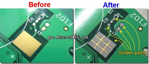
The solder paste printing process involves depositing a controlled amount of solder paste onto specific areas of the PCB, known as solder pads. This process is typically done using a stencil printer, which uses a laser-cut stencil to transfer the solder paste onto the PCB.
Stencil Design
The stencil is a thin metal sheet (usually stainless steel) with apertures that correspond to the solder pads on the PCB. The stencil design is crucial for achieving a consistent and accurate solder paste deposit. Factors to consider when designing a stencil include:
- Aperture size and shape
- Stencil thickness
- Aperture wall tapering
- Fiducial marks for alignment
Solder Paste Printing Equipment
Solder paste printing is typically performed using a stencil printer, which consists of the following components:
- Stencil frame and holder
- PCB support and clamping system
- Solder paste dispenser
- Vision system for alignment
- Squeegee blade for paste transfer
The stencil printer should be capable of precisely aligning the stencil with the PCB, dispensing the correct amount of solder paste, and achieving a consistent paste transfer across the entire PCB.
Solder Paste Printing Process Steps
The solder paste printing process involves the following steps:
- Stencil and PCB alignment using the vision system and fiducial marks
- Solder paste dispensing onto the stencil
- Squeegee blade movement across the stencil to transfer the paste onto the PCB
- PCB removal and inspection for defects
- Stencil cleaning to remove any residual solder paste
Proper control of the printing process parameters, such as squeegee pressure, speed, and angle, is essential for achieving a high-quality solder paste deposit.

Solder Paste Inspection and Defects
After the solder paste printing process, it is important to inspect the PCB for any defects or inconsistencies in the solder paste deposit. Some common solder paste printing defects include:
- Insufficient or excessive solder paste
- Bridging between solder pads
- Solder paste misalignment or offset
- Solder paste slumping or spreading
Solder paste inspection can be performed using various methods, such as:
- Visual inspection using magnification or microscopy
- 2D or 3D solder paste inspection (SPI) systems
- Laser triangulation or phase shift measurement techniques
Identifying and correcting solder paste printing defects early in the SMT assembly process can help to prevent component placement issues and improve the overall quality of the final product.

Factors Affecting Solder Paste Printing Quality
Several factors can influence the quality of the solder paste printing process, including:
- Solder paste properties (e.g., viscosity, particle size, flux activity)
- Stencil design and quality (e.g., aperture size, shape, and wall quality)
- Printing process parameters (e.g., squeegee pressure, speed, and angle)
- PCB and solder pad design (e.g., pad size, shape, and surface finish)
- Environmental conditions (e.g., temperature, humidity, and cleanliness)
Proper control and optimization of these factors are essential for achieving a consistent and reliable solder paste printing process.

Best Practices for Solder Paste Printing
To ensure a high-quality solder paste printing process, consider the following best practices:
- Use a high-quality solder paste with the appropriate properties for your application
- Design the stencil and PCB solder pads for optimal paste release and transfer
- Regularly maintain and calibrate the solder paste printing equipment
- Implement a robust process control and inspection system
- Train operators on proper handling and storage of solder paste and PCBs
- Monitor and control environmental conditions in the printing area
- Regularly clean and inspect the stencil for damage or contamination
By following these best practices and continuously improving the solder paste printing process, SMT assembly manufacturers can achieve higher yields, lower defect rates, and better overall product quality.
Frequently Asked Questions (FAQ)
1. What is the shelf life of solder paste, and how should it be stored?
Solder paste typically has a shelf life of 6-12 months when stored at a temperature of 0-10°C (32-50°F) in a refrigerator. It is important to allow the solder paste to reach room temperature before opening the container to prevent condensation and contamination. Once opened, solder paste should be used within 4-8 hours to ensure optimal performance.
2. How often should the stencil be cleaned during the solder paste printing process?
The frequency of stencil cleaning depends on various factors, such as the solder paste type, printing volume, and environmental conditions. As a general guideline, the stencil should be cleaned every 4-8 hours of continuous printing or after every shift change. However, more frequent cleaning may be necessary if defects or contamination are observed during the printing process.
3. What is the recommended solder paste printing speed and pressure?
The optimal solder paste printing speed and pressure depend on the specific solder paste, stencil design, and PCB characteristics. Typical printing speeds range from 20-150 mm/s, while squeegee pressures range from 0.2-1.0 kg/cm. It is important to optimize these parameters through experimentation and process validation to achieve the best solder paste printing results.
4. How can solder paste bridging defects be minimized?
Solder paste bridging defects can be minimized by optimizing the stencil design (e.g., reducing aperture size or increasing spacing between pads), adjusting the printing process parameters (e.g., reducing squeegee pressure or increasing speed), and ensuring proper PCB and stencil cleaning. Additionally, using a solder paste with the appropriate rheological properties and particle size can help to prevent bridging.
5. What are the advantages of using a step stencil for solder paste printing?
A step stencil is a stencil with varying thicknesses designed to accommodate different component heights or solder paste volume requirements on the same PCB. The advantages of using a step stencil include improved solder paste release for smaller apertures, reduced risk of component tombstoning, and better control over solder paste volume for different component types. Step stencils can help to optimize the solder paste printing process and improve the overall quality of the SMT assembly.
Conclusion
Solder paste printing is a critical process in SMT assembly that directly impacts the quality and reliability of the final product. By understanding the composition and properties of solder paste, designing an optimized stencil and PCB layout, and implementing proper process control and inspection, manufacturers can achieve a consistent and high-quality solder paste printing process. Continuous improvement and adherence to best practices are essential for staying competitive in the ever-evolving world of PCB assembly.


Leave a Reply