Introduction
Surface mount technology (SMT) has transformed how printed circuit boards (PCBs) are assembled and populated with components. First introduced in the 1960s, SMT gradually replaced the traditional through-hole technology (THT) approach and today accounts for over 90% of all PCB production.
SMT utilizes smaller, streamlined surface mount components along with automated assembly processes to achieve major benefits in density, efficiency, and reliability. However, the shift to microscopic SMT parts presented an array of manufacturing challenges requiring advanced techniques and tight process control.
This article provides an in-depth overview of SMT for PCBs. We’ll contrast the SMT and THT approaches, explain SMT components and packaging, discuss SMT assembly processes and equipment, and examine key factors for quality control.
SMT vs Through Hole Technology
Before SMT emerged, through-hole technology was the standard method of populating printed circuit boards with components. This involved inserting component leads through holes drilled in the PCB and soldering the leads on the opposite side to form both mechanical and electrical connections.
While effective, this approach consumed considerable board space to accommodate the holes and lead bending. Component placement was restricted by hole locations and lead lengths. Assembling boards manually was time consuming and anisotropic properties of plated through holes limited performance at high frequencies.
SMT revolutionized PCB assembly by:
- Placing components directly on surface pads instead of through holes
- Utilizing much smaller and lighter surface mount packages
- Enabling automation through specialized assembly machines
- Supporting miniaturization of circuitry and higher speeds
This transition brought dramatic improvements in density, throughput, quality, and reliability along with new manufacturing and inspection challenges.
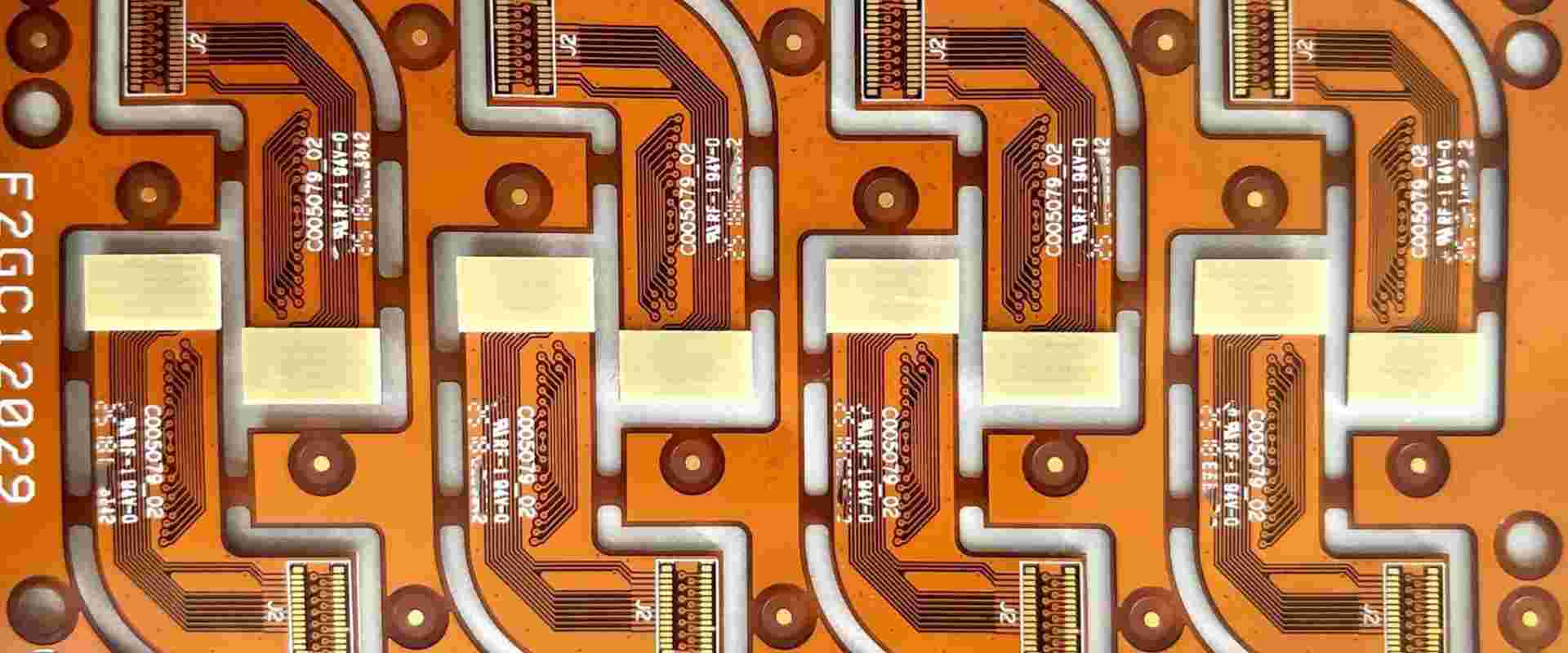
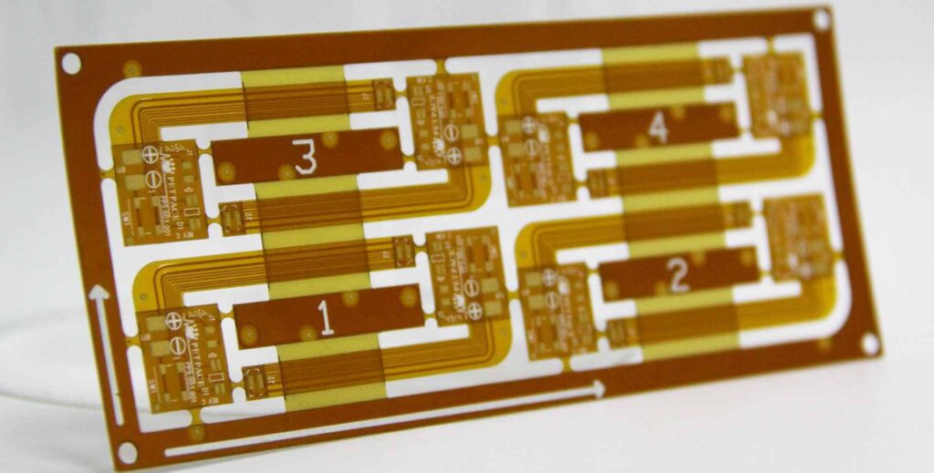
SMT Components
A wide array of specialized component packages are used in SMT to maximize density, interconnectability, and performance. Some common categories include:
Chip Components
- Resistors and capacitors – Tiny surface mount chips measuring just 1mm x 0.5mm with two pads
- Inductors – Small wirewound coils or multi-layer ceramic chips
- Noise suppression filters – Low pass filters in surface mount packages
Flat Lead Components
- Quad Flat Pack (QFP) – ICs with leads extending from four sides
- Small Outline IC (SOIC) – Rectangular ICs with leads on two sides
- Flat Pack (FP) – Square ICs with leads on four sides
Area Array Components
- Ball Grid Array (BGA) – BGA packages use an array of solder balls on bottom
- Chip Scale Packaging (CSP) -IC packages nearly identical in size to the silicon die
Connectors
- Board-to-board – High density connectors for stacking PCBs
- Board-to-cable – Low profile connectors without protruding pins
Specialty Components
- MEMS/Sensors – Microelectromechanical systems and sensors
- Bare die – Unpackaged IC dies attached directly to board
This extensive variety of component packages, lead configurations, sizes, and heights allows SMT assembly to support complex PCB population needs.
SMT Assembly Process Overview
Assembling a PCB via SMT involves sequentially attaching and soldering components to pads on the board surface. The basic SMT assembly process comprises the following key steps:
- Solder Paste Application – Solder paste is printed or jetted onto pads where components will be placed.
- Component Placement – Robotic pick and place machines precisely position components onto pads.
- Reflow Soldering – The assembly passes through a reflow oven melting solder and permanently attaching components.
- Cleaning – Flux residue is cleaned from the soldered assembly.
- Inspection – Automated optical inspection checks for defects and quality.
- Rework – If needed, misplaced components are removed and replaced by hand.
Additional steps like coating application, through-hole assembly, and functional test may also be integrated into the process depending on the specific PCB.
Next, we’ll look at these core SMT process steps in greater detail.
Solder Paste Application
Solder paste provides the solder alloy particles and flux medium needed to form solder joints during reflow. The paste must be deposited onto pads in a precise pattern matching the intended component layout prior to placement.
Printing is the most common method of solder paste application. Stencils perforated with apertures matching the PCB pad patterns are aligned over the board. Solder paste is dispensed along one edge of the stencil and a squeegee blade spreads it evenly, pressing paste through apertures onto the pads below.
Jetting is an alternative approach using metered solder paste dots dispensed from a nozzle. This eliminates stencils for greater flexibility but with lower throughput. Both printing and jetting machines feature optical alignment systems for accuracy.
The volume of paste deposited must be optimized based on factors like pad geometry, component size, alloy particle size, and reflow dynamics. Too little paste risks poor wetting while excess paste increases the chance of bridging between adjacent pads.
Component Placement
Pick and place machines populate PCBs by using vacuum nozzles to pick components from reels or trays and place them precisely onto pads with solder paste applied. Sophisticated computer vision aligns components and simultaneous multi-nozzle heads provide high throughput.
Flexible feeder racks allow loading diverse components for mixed SMT assembly. Nozzles and grippers handling the miniscule SMT parts must apply minimal force to avoid damage while ensuring accurate and secure placement.
High-speed pick-and-place systems can place over 100,000 components per hour with accuracy down to 0.05mm or better. This automation is critical for large-scale SMT production.
Reflow Soldering
Reflow is the process of heating an assembly to melt solder paste deposited on pads, wetting metal surfaces and forming reliable permanent solder joints with components.
The assembly passes through a reflow oven on a conveyor. Multiple heat zones raise temperatures progressively according to a thermal profile until reaching a peak above the melting point of the solder alloy. The assembly then cools gradually in later zones to solidify joints.
The reflow profile must be tuned for the solder alloy, paste fluxes, components, and board size to ensure excellent wetting and uniform heating without damaging sensitive parts. Common solder alloys like SAC305 melt around 217°C.
Infrared, convection, or vapor phase conveyorized ovens provide consistent results for high volume SMT reflow soldering. Smaller batches can use benchtop reflow tools.
Post Solder Cleaning
Solder paste contains flux with an activator to facilitate reflow. While essential for soldering, flux residues left on the PCB assembly can be problematic. Cleaning removes residual flux and other contaminants from the assembly.
The predominant solder flux cleaning methods include:
- Aqueous cleaning – Using detergent solutions to wash away flux residues
- Semi-aqueous cleaning – Combination of aqueous detergent and solvent cleaning
- Solvent cleaning – Applying solvents to dissolve flux residues
- Vapor phase cleaning – Condensing solvent vapors onto assembly to dissolve and rinse away residues
Cleanliness standards like IPC J-STD-001 spell out maximum permissible residue limits. Automated cleaning equipment provides consistency for high volume production.
Automated Optical Inspection (AOI)
Automated optical inspection (AOI) systems use high resolution cameras and image processing software to check assembles PCBs for defects which may cause functional or reliability issues.
Typical inspectable defects include:
- Missing components
- Misaligned components
- Tombstoned components
- Skewed components
- Insufficient or excess solder
- Solder bridges
- Paste printing imperfections
- Foreign object debris
AOI provides critical immediate feedback on assembly quality, avoiding wasted value-add steps when defects are detected early. Automated inspection also statistically quantifies the production process capability.
Rework
For some defective assemblies, it may be possible to rework and repair issues rather than scrap the board. BGA components in particular are difficult to remove and replace.
Rework requires specialized operators and tools. Vacuum pens, directed hot gas tools, and probing manipulate faulty components to be removed. Once extracted, new components can be placed back into the original position.
Minimizing rework instances through robust process control is preferable for throughput and quality. But rework does provide a second chance option before discarding expensive failed assemblies.
Key Factors for Quality SMT Assembly
Successfully implementing high quality SMT assembly necessitates tight control and continuous improvement across numerous process factors:
Materials
- Solder paste – Keeping paste refrigerated and monitoring viscosity and reflow response.
- Components – Managing moisture sensitivity and electrostatic discharge protection.
- Boards – Monitoring thickness, pad geometry, surface finish quality.
Machines
- Stencil printers – Monitoring paste deposition repeatability.
- Pick-and-place – Ensuring accuracy and precision over millions of cycles.
- Reflow ovens – Controlling thermal profiles and monitoring process windows.
- AOI systems – Qualifying image quality and analyzing statistical defect data.
Methods
- Process settings – Optimizing parameters like print pressure and reflow conveyor speed.
- Change control – Reviewing impacts of any component, board, or machine change.
- Training – Educating operators on proper setup, operation, and maintenance.
- Data analysis – Identifying patterns and correlations in quality data to guide improvements.
By holistically managing materials, machines, and methods, manufacturers can achieve excellent SMT quality and yields.
SMT vs Through Hole Assembly Comparison
| Metric | SMT | Through Hole |
|---|---|---|
| Component Size | 0402 chips (0.4mm x 0.2mm) <br> Fine pitch QFPs <br> 0.4mm BGA pitch | 5mm or larger pitch leaded components |
| Component Height | < 1mm | 10mm or taller component heights |
| Component Weight | < 1 gram | > 5 grams |
| Interconnect Density | High density – Thousands per inch^2 | Low density – Hundreds per inch^2 |
| Reliability | Excellent with proper process control | Prone to vibrational failures of leads and solder joints |
| Rework Difficulty | Very difficult, special tools required | Straightforward desoldering and lead replacement |
| ** prototyping** | Requires specialized prototyping processes | Easy hand assembly and soldering |
| Inspection Method | Automated optical inspection | Manual visual inspection |
| Lead Flexibility | None – Only available in packaged footprints | High flexibility in bending and trimming component leads |
Conclusion
Surface mount technology transformed electronics manufacturing over the past decades by enabling automated assembly of microscopic components. This drives unprecedented levels of miniaturization and efficiency.
However, the intricacies of SMT materials, machines, and methods demand tight process control and continuous improvement to achieve high yields and quality. When implemented successfully, SMT provides unmatched reliability at massive scales of production.
PCB designers now take the capabilities of SMT assembly for granted. But manufacturers must master nuances from solder paste printing to defect inspection to unlock the full potential of surface mount technology.
Frequently Asked Questions
What are the main benefits of SMT compared to through hole PCB assembly?
The principal benefits of SMT include improved density, speed, quality, reliability, and automation. SMT fits more components in less space, enables smaller products, allows faster automated assembly, and produces robust solder joint interconnections when properly implemented.
What is the most common SMT component package today?
The smallest passive chip components like 0402 or 0201 chips along with fine pitch QFP ICs and BGAs comprise over 75% of placements on a typical SMT assembly line. These components maximize space efficiency on crowded PCBs.
What is the key consideration when selecting components for an SMT PCB?
Components must be available in appropriate SMT packaged formats. This may require selecting SMT-specific component versions or substitutions for leaded versions. Components in ultra-fine pitch packages may also face placement and inspection challenges requiring assessment.
How accurate is automated SMT component placement on PCBs?
Top SMT pick-and-place machines achieve placement accuracies down to 0.05mm (50 microns). Vision-aided robotics continue improving as machine learning enhancement are applied. But tiny deviations can still cause defects.
What is the most challenging type of SMT component to inspect?
Bottom termination components like ball grid arrays (BGAs) cannot be visually inspected after placement. X-ray imaging is required to inspect solder joint quality underneath these hidden joints. Other components can at least be checked from the top side after soldering.


Leave a Reply