Introduction to PCB Milling
PCB milling is a subtractive manufacturing process used in the fabrication of printed circuit boards (PCBs). It involves the use of a computer-controlled milling machine to remove unwanted copper from a pre-laminated PCB substrate, leaving behind the desired electrical circuit pattern. This process is an alternative to traditional PCB Etching methods and offers several advantages, such as rapid prototyping, cost-effectiveness for small-batch production, and the ability to create complex geometries.
What is a PCB?
A printed circuit board (PCB) is a fundamental component in modern electronic devices. It is a flat board made of insulating materials, such as fiberglass or plastic, with conductive copper traces printed on its surface. These traces form the electrical connections between various components, such as resistors, capacitors, and Integrated Circuits (ICs), which are soldered onto the board. PCBs provide a compact and organized way to assemble electronic circuits, ensuring reliable connectivity and efficient signal transmission.
The Role of PCB Milling in PCB Fabrication
PCB milling plays a crucial role in the PCB fabrication process, particularly for prototyping and small-batch production. It offers several advantages over traditional PCB etching methods:
-
Rapid Prototyping: PCB milling allows for quick and efficient prototyping of PCB designs. The milling process can be completed in a matter of hours, enabling designers to test and refine their designs quickly.
-
Cost-Effectiveness: For small-batch production or one-off prototypes, PCB milling is often more cost-effective than traditional etching methods. It eliminates the need for expensive photomasks and chemical etching processes.
-
Flexibility: PCB milling machines can handle a wide range of PCB materials and thicknesses, allowing for greater design flexibility. They can also create complex geometries and fine details that may be challenging with traditional etching methods.
-
Environmental Friendliness: PCB milling is a dry process that does not involve the use of hazardous chemicals, making it a more environmentally friendly option compared to chemical etching.
The PCB Milling Process
The PCB milling process involves several steps, from preparing the PCB design files to the actual milling and post-processing of the board. Let’s take a closer look at each step:
Step 1: PCB Design and File Preparation
The first step in the PCB milling process is to create the PCB design using electronic design automation (EDA) software, such as KiCad, Eagle, or Altium Designer. The design includes the component placement, electrical connections, and routing of the copper traces.
Once the design is complete, it is exported in a format compatible with the milling machine’s software, such as Gerber or G-code files. These files contain the necessary information for the milling machine to interpret the design and generate the toolpaths for milling.
Step 2: PCB Material Selection and Preparation
The next step is to select the appropriate PCB substrate material. Common materials include FR-4 (fiberglass-reinforced epoxy laminate), Rogers, and polyimide. The choice of material depends on factors such as the intended application, operating frequency, and environmental conditions.
The selected PCB substrate is then cut to the desired size and shape using a cutting tool or laser cutter. It is important to ensure that the substrate is clean and free from dust or debris before proceeding to the milling stage.
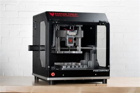
Step 3: Milling Machine Setup and Calibration
The PCB milling machine must be properly set up and calibrated before starting the milling process. This involves the following steps:
-
Tool Selection: Choose the appropriate milling tools based on the design requirements, such as the trace width, depth, and the type of material being milled. Common tools include end mills, drills, and engraving bits.
-
Tool Calibration: Calibrate the milling tools to ensure accurate positioning and depth control. This is typically done using a touch probe or by manually setting the tool offset values.
-
Workpiece Alignment: Align the PCB substrate on the milling machine’s work surface using alignment pins or a vacuum table to ensure precise positioning and prevent movement during milling.
-
Software Setup: Import the PCB design files into the milling machine’s software and set the appropriate milling parameters, such as spindle speed, feed rate, and depth of cut.
Step 4: PCB Milling
With the setup and calibration complete, the actual PCB milling process can begin. The milling machine follows the generated toolpaths to remove the unwanted copper from the PCB substrate, leaving behind the desired electrical circuit pattern.
The milling process typically involves multiple passes, with each pass removing a specific amount of material. The number of passes and the depth of cut depend on the design requirements and the thickness of the copper layer.
During the milling process, it is essential to monitor the machine for any signs of wear or breakage of the milling tools. Worn or damaged tools can lead to poor milling quality and may require replacement.
Step 5: Post-Processing and Inspection
After the milling process is complete, the PCB undergoes post-processing and inspection:
-
Cleaning: The milLED PCB is cleaned using compressed air or a soft brush to remove any debris or dust generated during the milling process.
-
Visual Inspection: The PCB is visually inspected for any defects, such as incomplete milling, shorts, or open circuits. Magnifying lenses or microscopes may be used for detailed inspection.
-
Electrical Testing: In some cases, electrical testing may be performed to ensure the continuity and isolation of the circuits. This can be done using a multimeter or a dedicated PCB Testing machine.
-
Surface Finishing: Depending on the application, the PCB may undergo additional surface finishing processes, such as solder mask application, silkscreen printing, or surface plating, to improve its durability and appearance.

Advantages of PCB Milling
PCB milling offers several advantages over traditional PCB etching methods:
-
Rapid Prototyping: PCB milling enables quick and efficient prototyping of PCB designs, allowing designers to test and refine their designs in a matter of hours.
-
Cost-Effectiveness: For small-batch production or one-off prototypes, PCB milling is often more cost-effective than traditional etching methods, as it eliminates the need for expensive photomasks and chemical etching processes.
-
Design Flexibility: PCB milling machines can handle a wide range of PCB materials and thicknesses, offering greater design flexibility. They can also create complex geometries and fine details that may be challenging with traditional etching methods.
-
Environmental Friendliness: PCB milling is a dry process that does not involve the use of hazardous chemicals, making it a more environmentally friendly option compared to chemical etching.
-
In-House Production: With a PCB milling machine, designers and engineers can fabricate PCBs in-house, reducing lead times and increasing control over the fabrication process.

Limitations of PCB Milling
While PCB milling offers many advantages, it also has some limitations:
-
Limited Production Volume: PCB milling is most suitable for prototyping and small-batch production. For high-volume production, traditional PCB etching methods are generally more efficient and cost-effective.
-
Tool Wear: The milling tools used in PCB milling are subject to wear and tear, which can affect the quality of the milled traces and require frequent tool replacements.
-
Limitations on Trace Width and Spacing: The minimum trace width and spacing achievable with PCB milling are generally larger compared to traditional etching methods. This is due to the physical limitations of the milling tools and the accuracy of the milling machine.
-
Substrate Material Restrictions: Some substrate materials, such as thin or flexible materials, may be challenging to mill due to their physical properties and the limitations of the milling machine.

Applications of PCB Milling
PCB milling finds applications in various industries and domains, including:
-
Electronics Prototyping: PCB milling is widely used for rapid prototyping of electronic circuits in research and development, allowing designers to quickly test and iterate their designs.
-
Education and Hobby Electronics: PCB milling machines are popular in educational institutions and among hobby electronics enthusiasts for creating custom PCBs for projects and experiments.
-
Aerospace and Defense: In the aerospace and defense industries, PCB milling is used for creating high-performance PCBs with complex geometries and strict tolerance requirements.
-
Medical Devices: PCB milling is employed in the fabrication of medical device electronics, where small-batch production and rapid prototyping are often required.
-
Automotive Electronics: PCB milling is used in the development and testing of automotive electronic systems, such as engine control units and infotainment systems.
Frequently Asked Questions (FAQ)
-
Q: What is the difference between PCB milling and PCB etching?
A: PCB milling is a subtractive manufacturing process that uses a computer-controlled milling machine to remove unwanted copper from a pre-laminated PCB substrate, leaving behind the desired electrical circuit pattern. In contrast, PCB etching is a chemical process that involves selectively removing unwanted copper using etchants, such as ferric chloride or ammonium persulfate, while protecting the desired circuit pattern with a photoresist mask. -
Q: What materials can be used for PCB milling?
A: Common materials used for PCB milling include FR-4 (fiberglass-reinforced epoxy laminate), Rogers, and polyimide. The choice of material depends on factors such as the intended application, operating frequency, and environmental conditions. -
Q: What is the minimum trace width and spacing achievable with PCB milling?
A: The minimum trace width and spacing achievable with PCB milling depend on the capabilities of the milling machine and the milling tools used. Typically, PCB milling can achieve trace widths and spacing in the range of 0.1 mm to 0.5 mm, although more advanced machines may be capable of finer resolutions. -
Q: How long does it take to mill a PCB?
A: The time required to mill a PCB depends on various factors, such as the complexity of the design, the size of the board, and the capabilities of the milling machine. Simple designs can be milled in a matter of minutes, while more complex designs may take several hours. -
Q: Can PCB milling be used for high-volume production?
A: PCB milling is generally more suitable for prototyping and small-batch production. For high-volume production, traditional PCB etching methods are often more efficient and cost-effective due to their ability to process multiple boards simultaneously and the lower cost per unit at higher volumes.
Conclusion
PCB milling is a versatile and efficient method for fabricating printed circuit boards, particularly for prototyping and small-batch production. It offers several advantages over traditional PCB etching methods, such as rapid prototyping, cost-effectiveness, design flexibility, and environmental friendliness.
By understanding the PCB milling process, its advantages, limitations, and applications, designers and engineers can make informed decisions when choosing the most suitable fabrication method for their projects. As technology advances, PCB milling machines are becoming increasingly capable and affordable, making them an attractive option for a wide range of industries and applications.


Leave a Reply