The Importance of PCB Design
PCB design plays a vital role in the success of an electronic device. A well-designed PCB ensures that the device functions as intended, is reliable, and can be manufactured efficiently. Some of the key reasons why PCB design is important include:
-
Functionality: A properly designed PCB ensures that all components are connected correctly and that the circuit functions as intended.
-
Reliability: Good PCB design practices, such as proper component placement and trace routing, can help minimize signal interference and improve the overall reliability of the device.
-
Manufacturing: A well-designed PCB is easier to manufacture, which can reduce production costs and lead times.
-
Performance: Optimal component placement and trace routing can help minimize signal loss and improve the overall performance of the device.
The PCB Design Process
The PCB design process typically involves several steps, each of which plays a crucial role in the final design. These steps include:
Schematic Design
The first step in the PCB design process is to create a schematic diagram of the circuit. This involves selecting the appropriate components and defining how they are connected. The schematic design is typically created using electronic design automation (EDA) software, such as Altium Designer or KiCad.
Component Placement
Once the schematic design is complete, the next step is to place the components on the PCB. This involves determining the optimal location for each component based on factors such as signal integrity, thermal management, and manufacturability. Component placement is typically done using PCB layout software.
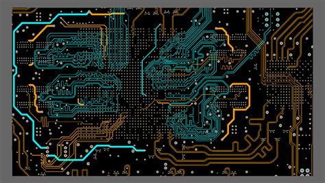
Trace Routing
After the components are placed, the next step is to route the traces that connect them. This involves creating a network of copper traces on the PCB that carry signals between the components. Trace routing is typically done using PCB layout software and requires careful consideration of factors such as signal integrity, impedance matching, and crosstalk.
Design Rule Checking (DRC)
Once the initial PCB layout is complete, the next step is to perform a design rule check (DRC). This involves checking the design against a set of predefined rules to ensure that it meets all necessary requirements for manufacturing and functionality. DRC helps identify potential issues such as short circuits, insufficient clearances, and incomplete connections.
Gerber File Generation
The final step in the PCB design process is to generate the Gerber files that will be used for manufacturing. Gerber files are a standard format used by PCB manufacturers to create the physical PCB. They contain all the necessary information about the PCB layout, including the location of components, traces, and drill holes.

PCB Design Considerations
When designing a PCB, there are several key considerations that must be taken into account to ensure the best possible performance and reliability. These include:
Signal Integrity
Signal integrity refers to the quality of the signals transmitted through the PCB. It is affected by factors such as trace length, impedance matching, and crosstalk. To ensure good signal integrity, designers must carefully consider the placement of components and the routing of traces.
Thermal Management
Thermal management refers to the ability of the PCB to dissipate heat generated by the components. Poor thermal management can lead to overheating, which can cause components to fail prematurely. To ensure good thermal management, designers must consider factors such as component placement, copper pour, and the use of thermal vias.
Electromagnetic Compatibility (EMC)
Electromagnetic compatibility (EMC) refers to the ability of the PCB to operate without causing or being affected by electromagnetic interference (EMI). EMI can cause signal degradation and other issues that can affect the performance and reliability of the device. To ensure good EMC, designers must consider factors such as component placement, trace routing, and the use of shielding.
Manufacturability
Manufacturability refers to the ease with which the PCB can be manufactured. A design that is difficult to manufacture can lead to increased production costs and longer lead times. To ensure good manufacturability, designers must consider factors such as component placement, trace width and spacing, and the use of vias.

PCB Layout Techniques
There are several techniques that designers can use to optimize the layout of a PCB. These include:
Ground Planes
Ground planes are large areas of copper on the PCB that are connected to ground. They provide a low-impedance return path for signals and help reduce EMI. Ground planes also help improve signal integrity by reducing crosstalk and providing a stable reference voltage.
Power Planes
Power planes are similar to ground planes but are used to distribute power to the components on the PCB. They provide a low-impedance path for current and help reduce voltage drop across the board. Power planes also help reduce EMI by providing a low-impedance return path for high-frequency signals.
Trace Routing Techniques
There are several techniques that designers can use to optimize the routing of traces on the PCB. These include:
- Daisy-chaining: Daisy-chaining involves connecting components in series, which can help reduce the number of vias and improve signal integrity.
- Serpentine routing: Serpentine routing involves routing traces in a zigzag pattern, which can help match trace lengths and reduce crosstalk.
- Differential pair routing: Differential pair routing involves routing two traces in close proximity to each other, which can help reduce EMI and improve signal integrity.

PCB Design Software
There are several software tools available for PCB design, ranging from free and open-source options to high-end commercial packages. Some of the most popular PCB design software tools include:
| Software | Description | Price |
|---|---|---|
| Altium Designer | High-end PCB design software with advanced features and a steep learning curve | $$$$ |
| KiCad | Free and open-source PCB design software with a growing user community | Free |
| Eagle | Popular PCB design software with a free version available for small projects | $$ |
| OrCAD | Comprehensive PCB design software with a focus on advanced simulation and analysis | $$$ |
FAQ
What is the difference between a schematic and a PCB layout?
A schematic is a diagram that shows the electrical connections between components, while a PCB layout is a physical representation of the circuit on a board. The schematic is used to create the PCB layout, which includes the placement of components and routing of traces.
What is the purpose of a ground plane?
A ground plane is a large area of copper on the PCB that is connected to ground. It provides a low-impedance return path for signals and helps reduce EMI. Ground planes also help improve signal integrity by reducing crosstalk and providing a stable reference voltage.
What is the difference between a via and a through-hole?
A via is a small hole in the PCB that is used to connect traces on different layers of the board. A through-hole is a larger hole that is used to mount components on the board. Through-holes are typically used for components that require mechanical stability, such as connectors and switches.
What is the difference between a power plane and a ground plane?
A power plane is similar to a ground plane but is used to distribute power to the components on the PCB. It provides a low-impedance path for current and helps reduce voltage drop across the board. A ground plane, on the other hand, is connected to ground and provides a low-impedance return path for signals.
What is the purpose of a design rule check (DRC)?
A design rule check (DRC) is a process of checking the PCB layout against a set of predefined rules to ensure that it meets all necessary requirements for manufacturing and functionality. DRC helps identify potential issues such as short circuits, insufficient clearances, and incomplete connections. It is an important step in the PCB design process to ensure the final product is reliable and manufacturable.
Conclusion
PCB design and layout is a critical step in the development of electronic devices. It involves the placement of components, routing of traces, and creation of a final design file that can be sent for manufacturing. A well-designed PCB ensures that the device functions as intended, is reliable, and can be manufactured efficiently.
When designing a PCB, there are several key considerations that must be taken into account, including signal integrity, thermal management, electromagnetic compatibility, and manufacturability. Designers can use various techniques such as ground planes, power planes, and trace routing techniques to optimize the layout of the PCB.
There are several software tools available for PCB design, ranging from free and open-source options to high-end commercial packages. Choosing the right software depends on factors such as project complexity, budget, and user preference.
Overall, PCB design and layout is a complex process that requires careful planning and attention to detail. By following best practices and using the right tools and techniques, designers can create high-quality PCBs that meet the needs of their projects and customers.


Leave a Reply