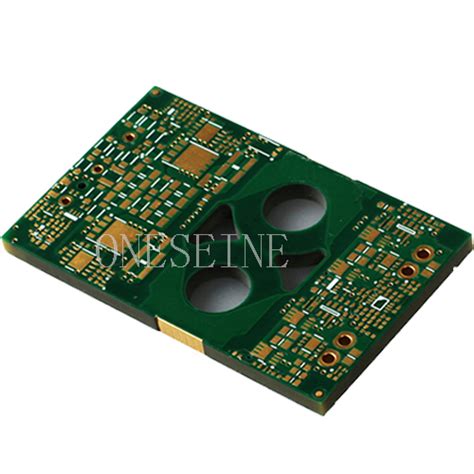
Introduction to Heavy Copper PCB
A Heavy Copper PCB, also known as a thick copper PCB or high current PCB, is a type of printed circuit board that utilizes thicker copper traces than standard PCBs. These boards are designed to handle higher currents and offer superior thermal management, making them ideal for power electronics, automotive applications, and other high-power systems.
What Makes a PCB a Heavy Copper PCB?
The primary distinguishing factor of a heavy copper PCB is the thickness of its copper traces. While standard PCBs typically feature copper traces ranging from 0.5 oz to 2 oz per square foot (17 to 68 μm), heavy copper PCBs can have copper thicknesses ranging from 3 oz to 20 oz per square foot (102 to 680 μm) or even more in some cases.
| Copper Weight (oz/ft²) | Thickness (μm) |
|---|---|
| 0.5 | 17 |
| 1 | 34 |
| 2 | 68 |
| 3 | 102 |
| 4 | 136 |
| 6 | 203 |
| 8 | 272 |
| 10 | 339 |
| 12 | 407 |
| 16 | 543 |
| 20 | 678 |
Benefits of Using Heavy Copper PCBs
-
Higher Current Carrying Capacity: The thicker copper traces in heavy copper PCBs allow them to carry higher currents without overheating or suffering from voltage drops. This makes them suitable for power-intensive applications.
-
Improved Thermal Management: The increased copper thickness also enhances the PCB’s ability to dissipate heat, reducing the risk of thermal damage to components and increasing the overall reliability of the system.
-
Lower Resistance: Thicker copper traces have lower electrical resistance, which minimizes power losses and improves the efficiency of the circuit.
-
Better Mechanical Stability: Heavy copper PCBs offer greater mechanical stability and durability compared to standard PCBs, making them more resistant to vibrations and physical stresses.
Applications of Heavy Copper PCBs
Power Electronics
Heavy copper PCBs are widely used in power electronics applications, such as:
- Power supplies
- Inverters
- Motor drives
- Uninterruptible power supplies (UPS)
- Solar power systems
In these applications, heavy copper PCBs enable efficient power delivery, effective heat dissipation, and reliable operation under high-current conditions.
Automotive Electronics
The automotive industry increasingly relies on heavy copper PCBs for various applications, including:
- Electric vehicle battery management systems
- Engine control units (ECUs)
- Power steering systems
- Lighting systems
- Infotainment systems
Heavy copper PCBs provide the necessary current-carrying capacity, thermal management, and durability required in the demanding automotive environment.
Industrial Equipment
Heavy copper PCBs find extensive use in industrial equipment, such as:
- Welding machines
- CNC machines
- Robotics
- Motor controllers
- Power distribution systems
The high-power requirements and harsh operating conditions in industrial settings make heavy copper PCBs an ideal choice for these applications.
Telecommunications
In the telecommunications industry, heavy copper PCBs are used in:
- Base stations
- Antenna systems
- Power amplifiers
- Switching equipment
The increased copper thickness ensures reliable power delivery and effective heat dissipation, which are critical for maintaining the performance and longevity of telecommunications equipment.

Designing Heavy Copper PCBs
Considerations for Heavy Copper PCB Design
When designing heavy copper PCBs, several key factors must be considered:
-
Copper Thickness Selection: Choose the appropriate copper thickness based on the current-carrying requirements and thermal management needs of the application.
-
Trace Width and Spacing: Ensure that the trace widths and spacing are adequate for the chosen copper thickness to avoid manufacturing issues and maintain proper electrical isolation.
-
Thermal Management: Incorporate thermal management techniques, such as the use of thermal vias, heat sinks, or copper pours, to effectively dissipate heat generated by high-power components.
-
Layer Stack-up: Optimize the layer stack-up to minimize signal integrity issues and ensure proper power distribution.
-
Manufacturing Constraints: Consider the manufacturing capabilities of your PCB fabrication partner, as not all manufacturers have the expertise or equipment to produce heavy copper PCBs.
Heavy Copper PCB Design Guidelines
To ensure the successful design and manufacturing of heavy copper PCBs, follow these guidelines:
-
Use appropriate trace widths: Calculate the required trace widths based on the expected current, copper thickness, and temperature rise using industry-standard formulas or design tools.
-
Maintain proper trace spacing: Ensure sufficient spacing between traces to prevent electrical shorts and maintain signal integrity. The spacing requirements may increase with thicker copper traces.
-
Incorporate thermal relief pads: Use thermal relief pads for component connections to minimize thermal stress and improve solderability.
-
Use thermal vias: Incorporate thermal vias to transfer heat from the PCB surface to the inner layers or the opposite side of the board, enhancing overall thermal dissipation.
-
Consider copper balancing: Ensure that the copper distribution across the PCB is balanced to minimize warping and improve manufacturing yield.
-
Collaborate with your PCB manufacturer: Work closely with your PCB fabrication partner to ensure that your design is manufacturable and optimized for heavy copper PCB production.

Manufacturing Heavy Copper PCBs
Heavy Copper PCB Manufacturing Process
The manufacturing process for heavy copper PCBs is similar to that of standard PCBs but with some additional considerations:
-
Copper Plating: The desired copper thickness is achieved through an electroplating process, where additional copper is deposited onto the base copper layer.
-
Etching: The plated copper is then etched to create the desired trace patterns. The etching process may take longer for heavy copper PCBs due to the increased copper thickness.
-
Lamination: The etched copper layers are laminated together with insulating material to form the complete PCB stack-up.
-
Drilling and Plating: Holes are drilled through the PCB, and the walls of the holes are plated with copper to create electrical connections between layers.
-
Surface Finish: A surface finish, such as HASL, ENIG, or OSP, is applied to protect the exposed copper and improve solderability.
Challenges in Heavy Copper PCB Manufacturing
Manufacturing heavy copper PCBs presents some unique challenges compared to standard PCBs:
-
Longer Plating and Etching Times: The increased copper thickness requires longer plating and etching times, which can impact production throughput and costs.
-
Handling and Warping: Thicker copper layers can make the PCB more prone to warping during the manufacturing process, requiring careful handling and specialized equipment.
-
Drill Bit Wear: Drilling through thicker copper layers can cause increased wear on drill bits, necessitating more frequent tool changes and maintenance.
-
Specialized Equipment: Manufacturing heavy copper PCBs may require specialized equipment, such as high-capacity plating tanks and high-speed drills, which not all PCB manufacturers possess.

Testing and Quality Control for Heavy Copper PCBs
To ensure the reliability and performance of heavy copper PCBs, stringent testing and quality control measures are essential:
-
Visual Inspection: A thorough visual inspection is performed to check for any surface defects, such as scratches, pits, or discoloration.
-
Electrical Testing: Electrical tests, such as continuity and isolation tests, are conducted to verify the integrity of the electrical connections and the absence of short circuits.
-
Microsectioning: Microsectioning involves cross-sectioning the PCB and examining it under a microscope to assess the quality of the plating, lamination, and drilling processes.
-
Thermal Cycling: Thermal cycling tests expose the PCB to alternating high and low temperatures to evaluate its ability to withstand thermal stresses and maintain its structural integrity.
-
High-Current Testing: High-current tests are performed to ensure that the heavy copper PCB can handle the specified current levels without overheating or suffering from voltage drops.
-
Accelerated Life Testing: Accelerated life testing subjects the PCB to extreme conditions, such as high temperature and humidity, to assess its long-term reliability and identify any potential failure modes.
By implementing these testing and quality control measures, manufacturers can ensure that heavy copper PCBs meet the required performance standards and can withstand the demands of their intended applications.
FAQ
1. What is the difference between a heavy copper PCB and a standard PCB?
The main difference between a heavy copper PCB and a standard PCB lies in the thickness of the copper traces. Heavy copper PCBs have copper traces that are significantly thicker than those in standard PCBs, typically ranging from 3 oz to 20 oz per square foot (102 to 680 μm) or more. This increased copper thickness enables heavy copper PCBs to carry higher currents, offer better thermal management, and provide improved mechanical stability.
2. What are the main applications for heavy copper PCBs?
Heavy copper PCBs find applications in various industries where high-power handling and efficient thermal management are critical. Some of the main applications include:
– Power electronics: Power supplies, inverters, motor drives, and solar power systems
– Automotive electronics: Electric vehicle battery management systems, engine control units, and power steering systems
– Industrial equipment: Welding machines, CNC machines, robotics, and motor controllers
– Telecommunications: Base stations, antenna systems, power amplifiers, and switching equipment
3. What are the key considerations when designing heavy copper PCBs?
When designing heavy copper PCBs, several key factors must be considered, such as:
– Selecting the appropriate copper thickness based on current-carrying requirements and thermal management needs
– Ensuring adequate trace widths and spacing for the chosen copper thickness
– Incorporating thermal management techniques, like thermal vias, heat sinks, or copper pours
– Optimizing the layer stack-up for proper power distribution and signal integrity
– Considering the manufacturing capabilities of the PCB fabrication partner
4. How does the manufacturing process differ for heavy copper PCBs compared to standard PCBs?
The manufacturing process for heavy copper PCBs is similar to that of standard PCBs but with some additional considerations. The desired copper thickness is achieved through an electroplating process, followed by etching to create the trace patterns. The etching process may take longer for heavy copper PCBs due to the increased copper thickness. The PCB stack-up is then laminated, drilled, and plated, and a surface finish is applied. Manufacturing heavy copper PCBs may require specialized equipment and longer processing times compared to standard PCBs.
5. What testing and quality control measures are important for heavy copper PCBs?
To ensure the reliability and performance of heavy copper PCBs, various testing and quality control measures are employed, including:
– Visual inspection for surface defects
– Electrical testing for continuity and isolation
– Microsectioning to assess plating, lamination, and drilling quality
– Thermal cycling to evaluate the PCB’s ability to withstand thermal stresses
– High-current testing to ensure the PCB can handle specified current levels without issues
– Accelerated life testing to assess long-term reliability under extreme conditions
These measures help guarantee that heavy copper PCBs meet the required performance standards and can withstand the demands of their intended applications.
Conclusion
Heavy copper PCBs offer a robust solution for applications that require high current-carrying capacity, efficient thermal management, and improved mechanical stability. By utilizing thicker copper traces, these PCBs can handle the demands of power electronics, automotive systems, industrial equipment, and telecommunications infrastructure.
Designing and manufacturing heavy copper PCBs involves careful consideration of factors such as copper thickness, trace widths and spacing, thermal management, and layer stack-up optimization. Close collaboration with experienced PCB fabrication partners is essential to ensure the successful production of high-quality heavy copper PCBs.
Through rigorous testing and quality control measures, manufacturers can guarantee the reliability and performance of heavy copper PCBs in their intended applications. As technology continues to advance and the demand for high-power electronics grows, heavy copper PCBs will likely play an increasingly important role in shaping the future of various industries.


Leave a Reply