Introduction
In the world of electronics, printed circuit boards (PCBs) play a crucial role in interconnecting various components and enabling the flow of electrical signals. At the heart of a PCB lies a critical component known as the substrate. This substrate serves as the foundation upon which the intricate circuitry and components are mounted and interconnected. Understanding the nature and properties of the substrate is essential for designing and manufacturing high-quality and reliable PCBs.
What is a Substrate?
A substrate in a PCB is a thin, rigid, insulating material that provides the base layer for the conductive traces and components. It is a crucial component that supports and insulates the electrical connections while offering mechanical stability to the overall PCB assembly. The substrate acts as a dielectric, preventing the conduction of electricity between adjacent conductive layers.
Substrate Materials
Various materials can be used as substrates in PCB manufacturing, each with its own unique properties and characteristics. The most common substrate materials include:
- FR-4 (Flame Retardant 4): This is the most widely used substrate material in the PCB industry. FR-4 is a composite material made of woven fiberglass reinforced with an epoxy resin. It offers excellent mechanical strength, electrical insulation, and heat resistance, making it suitable for a wide range of applications.
- Polyimide: Polyimide substrates are known for their exceptional thermal stability and resistance to high temperatures. They are commonly used in applications where PCBs are exposed to extreme temperature environments, such as aerospace, military, and automotive industries.
- Ceramic: Ceramic substrates, such as alumina (Al2O3) and aluminum nitride (AlN), are highly resistant to high temperatures and offer excellent electrical insulation properties. They are often used in high-frequency and high-power applications, as well as in harsh environments.
- Rogers Materials: These are engineered materials specifically designed for high-frequency and microwave applications. Rogers materials, such as RO4003C and RT/duroid, offer low dielectric loss and consistent electrical performance over a wide range of frequencies.
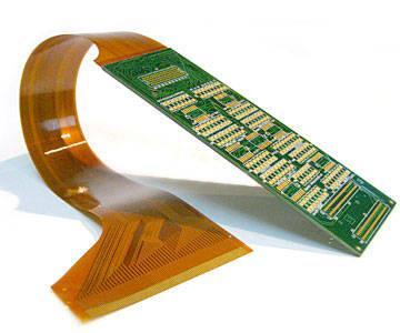
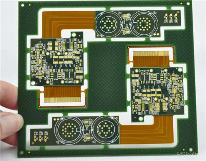
- Flex Materials: Flexible substrates, such as polyimide and polyester films, are used in the manufacturing of flexible and rigid-flex PCBs. These substrates allow for unique form factors and applications where flexibility is a requirement.
Each substrate material has its own unique set of properties, including dielectric constant, dissipation factor, thermal conductivity, and coefficient of thermal expansion (CTE). The choice of substrate material is determined by the specific requirements of the application, such as operating frequency, power handling capabilities, environmental conditions, and mechanical stress.
Substrate Layers and Construction
A PCB substrate can be composed of multiple layers, each serving a specific purpose. The most common layer configurations include:
- Single-layer: This is the simplest form of a PCB substrate, consisting of a single layer of conductive material (typically copper) on one side of the insulating substrate.
- Double-layer: In a double-layer substrate, conductive layers are present on both sides of the insulating material, with plated-through holes (PTHs) providing electrical connections between the two layers.
- Multi-layer: Multi-layer substrates consist of multiple conductive layers separated by insulating layers. These layers are interconnected using PTHs or vias, allowing for more complex circuit designs and higher component densities.
The construction of a multi-layer substrate typically involves the following steps:
- Lamination: Individual layers of conductive material (typically copper foil) and insulating material (pre-preg or core) are stacked and bonded together under high temperature and pressure, forming a solid laminate structure.
- Drilling: Holes are drilled through the laminate to create PTHs or vias for interconnecting the conductive layers.
- Plating: The drilled holes are plated with conductive materials, such as copper, to create electrical connections between the layers.
- Patterning: The conductive layers are etched or removed selectively to create the desired circuit patterns and interconnections.
- Finishing: Additional processes, such as solder mask application and surface finishes, may be applied to protect the circuitry and facilitate assembly.
The number of layers and the specific construction techniques used in a PCB substrate depend on the complexity of the design, signal integrity requirements, and manufacturing capabilities.
Substrate Properties and Considerations
When selecting a substrate material and designing a PCB, several properties and considerations must be taken into account:
- Dielectric Constant (Dk): The dielectric constant, or permittivity, of a substrate material determines the propagation speed of electrical signals through the material. Lower Dk values are desirable for high-frequency applications to minimize signal distortion and improve signal integrity.
- Dissipation Factor (Df): The dissipation factor, or loss tangent, represents the amount of energy lost as heat within the substrate material during signal transmission. Lower Df values are preferred to minimize signal attenuation and power losses.
- Thermal Conductivity: The ability of a substrate material to conduct and dissipate heat is crucial for applications involving high power densities or operating temperatures. Materials with higher thermal conductivity are preferred in such cases.
- Coefficient of Thermal Expansion (CTE): The CTE determines the extent to which a material expands or contracts with changes in temperature. A mismatch in CTE between the substrate and other components can lead to mechanical stress and potential delamination or cracking.
- Moisture Absorption: Some substrate materials are prone to absorbing moisture, which can adversely affect their electrical and mechanical properties. Materials with low moisture absorption are preferred for applications in humid or harsh environments.
- Surface Roughness: The surface roughness of the substrate can impact the adhesion of conductive layers and the reliability of interconnections. Smooth surfaces are generally preferred for high-frequency and high-density interconnect (HDI) applications.
- Fabrication Capabilities: The choice of substrate material should also consider the manufacturing capabilities and limitations of the PCB fabrication process, such as drilling, plating, and lamination techniques.
By carefully considering these properties and matching them with the specific requirements of the application, designers can optimize the performance, reliability, and cost-effectiveness of the PCB.
Substrate Trends and Advancements
As electronic devices become more compact, powerful, and operate at higher frequencies, the demand for advanced substrate materials and technologies continues to grow. Some notable trends and advancements in the field of PCB substrates include:
- Low-loss Materials: The development of substrate materials with lower dielectric loss and dissipation factors is crucial for high-frequency and high-speed applications, such as 5G communications, radar, and millimeter-wave systems.
- High-density Interconnect (HDI) Substrates: HDI substrates feature finer line and space geometries, higher component densities, and smaller vias, enabling the miniaturization of electronic devices while maintaining high performance.
- Embedded Components: Advancements in substrate technologies allow for the embedding of passive components, such as capacitors and resistors, directly within the substrate layers, reducing the overall footprint and enabling higher functional densities.
- Thermal Management Solutions: As power densities increase, the need for effective thermal management solutions has become more prominent. Substrates with improved thermal conductivity, integrated heat sinks, or embedded cooling channels are being developed to address this challenge.
- Flexible and Stretchable Substrates: The demand for wearable electronics, flexible displays, and unconventional form factors has driven the development of flexible and stretchable substrates, enabling new applications and design possibilities.
- Environmentally Friendly Materials: There is a growing emphasis on developing substrate materials that are more environmentally friendly and comply with regulations related to hazardous substances, such as the Restriction of Hazardous Substances (RoHS) directive.
These trends and advancements in substrate technologies are driven by the ever-increasing demands for higher performance, miniaturization, and reliability in electronic devices across various industries, including consumer electronics, telecommunications, aerospace, and automotive.
Frequently Asked Questions (FAQs)
- What is the difference between a substrate and a PCB? A substrate is the insulating base material upon which the conductive layers and components are mounted in a PCB. The PCB itself is the complete assembly, which includes the substrate, conductive layers, and various components.
- Why is the choice of substrate material important in PCB design? The substrate material plays a crucial role in determining the electrical, thermal, and mechanical properties of the PCB. Selecting the appropriate substrate material ensures optimal performance, reliability, and compatibility with the application requirements.
- Can a PCB have multiple substrate layers? Yes, PCBs can have multiple substrate layers, known as multi-layer substrates. These layers are bonded together and interconnected using plated-through holes (PTHs) or vias, allowing for more complex circuit designs and higher component densities.
- What is the difference between FR-4 and polyimide substrates? FR-4 is a composite material made of woven fiberglass reinforced with an epoxy resin, while polyimide is a polymer material. Polyimide substrates are known for their exceptional thermal stability and resistance to high temperatures, making them suitable for applications with extreme temperature environments.
- What is the purpose of using a low-loss substrate material in high-frequency applications? In high-frequency applications, low-loss substrate materials with low dielectric loss and dissipation factors are preferred. These materials minimize signal attenuation and power losses, ensuring better signal integrity and higher performance at high frequencies.
By understanding the role and properties of substrates in PCB design and manufacturing, engineers and designers can make informed decisions to optimize the performance, reliability, and cost-effectiveness of their electronic products.


Leave a Reply