Introduction
A PCB (printed circuit board) stackup refers to the sequence and thickness of conductive copper layers and insulating dielectric materials that make up a multilayer PCB. The stackup defines the structure of the PCB and is a critical factor impacting the performance and manufacturability of the board. Careful stackup design is required to meet electrical, thermal, mechanical and high speed signal integrity requirements.
Some key points about PCB stackups:
- Multilayer PCBs consist of alternate layers of copper and dielectric materials bonded together into a single board.
- Number of conductive layers can range from 2 to over 30+ in complex boards. More layers provide increased routing capacity.
- Stackup determines number of layers, dielectric materials used, copper weights, and sequence of layers.
- Stackup design involves managing tradeoffs between electrical performance, thermal dissipation, manufacturability, reliability and cost.
- Key elements of stackup design are layer count, dielectric materials, copper weights, lamination technique, impedances, thickness etc.
- Careful modeling, simulation and design rule checks are needed to optimize stackup configuration.
Functions of Different Layers
The different conductive layers in the PCB stackup perform specialized functions:
Signal Layers
- Used for routing traces that carry signals between components on the PCB.
- Signal layers are usually inner layers in multilayer boards, protected from external EMI.
- Critical signals with high speed or noise sensitivity are routed on inner low noise reference planes.
Ground Layer
- Serves as a low impedance return path for signals to prevent noise coupling.
- Provides shielding from EMI, aids thermal dissipation. Often placed next to a signal layer.
- Split ground planes help isolate noise sensitive signals from noisy digital circuits.
Power Layer
- Distributes power from the source to components with minimal voltage drop.
- Prevents noise coupling between power distribution and signal layers.
- May be further split into analog and digital power planes to isolate noise.
High Speed Signals
- Routed on inner layers adjacent to ground planes for controlled impedance environment.
- May use wider traces, thicker copper, microstrip traces, buried vias etc. to manage lengths, impedance, isolation etc.
External Layers
- Outer layers allow mounting of components, connectors, vias etc.
- Often reserved for low speed signals, power distribution, component pads etc.
- Top layer allows marking of assembly details like part numbers, text, patterns etc.
Key Stackup Design Considerations
Several electrical, thermal, mechanical and high speed design factors need to be addressed in the stackup design:
Layer Count
- Higher layer counts provide increased routing capacity but add cost.
- Layer count depends on board complexity, component density, high speed traces etc.
- Typical layer counts are 4 to 16 layers for most boards. Some complex boards use 20+ layers.
Signal Routing
- Related signals should be routed together on the same layer for easier trace length matching.
- Group signals with similar characteristics – high speed, noise sensitive, single-ended, differential etc.
- Assign entire layers for critical nets like DDR memory buses for isolation.
Reference Planes
- Add ground and power planes adjacent to signal layers for controlled impedance environment.
- Place ground planes next to high speed or noise sensitive traces for shielding EMI.
- Use complete unbroken planes for low impedance current return paths.
Dielectric Materials
- Material properties like Dk affect impedance, propagation delay, losses, EMI etc.
- Low Dk, low loss materials enhance high frequency performance but cost more.
- FR-4 glass epoxy is suitable for most cost sensitive boards operating under 5 GHz.
- High frequency boards above 5 GHz use advanced materials like polyimide, hydrocarbon, PTFE etc.
Copper Thickness
- Thicker copper reduces conductor losses, spreads heat better. But adds cost.
- Typical thicknesses are 1 oz (35 μm) for outer layers and 0.5 oz (17 μm) for inner layers.
- High current layers like power distribution use 2 oz (70 μm) or more copper thickness.
High Speed Design
- Match trace lengths, spacings, impedances for differential pairs.
- Use buried vias, blind vias, back drilling techniques to manage via stubs.
- Allow for isolation bands between critical nets to prevent crosstalk.
- Model propagation delays to optimize trace lengths, termination schemes.
- Simulate and de-embed S-parameter, TDR, eye diagram models.
Thermal Issues
- Wider copper planes and thicker metallization help dissipate heat.
- Strategic placement of ground and power planes conducts heat away from hot spots.
- Thermal vias help conduct heat vertically from inner layers to external layers.
- Use thermally conductive dielectric materials like ceramic filled polymers.
Manufacturing Constraints
- Standard layer count and prepregs suited for lamination process selected.
- Minimum dielectric thickness requirements maintained for reliable multilayer bonding.
- Aspect ratio limits set for high density microvias.
- Panel utilization optimized for board dimensions.
Typical PCB Stackup Configurations
Here are some commonly used stackup configurations in multilayer PCB designs:
4 Layer Board
- Often optimal balance of cost, electrical performance, thickness.
- Typical stackup: Signal-GND-PWR-Signal
- GND and PWR reference planes sandwich inner signals.
- Alternate for high speed: Signal-PWR-GND-Signal
6 Layer Board
- Allows for additional routing capacity over 4 layers.
- Typical stackup: Signal-GND-PWR-Signal-PWR-Signal
- Dedicated power distribution layer added.
8 Layer Board
- Supports more complex routing and isolation for high speed.
- Typical stackup: Signal-GND-Signal-PWR-Signal-GND-PWR-Signal
- Additional signal routing layer inserted along with second power plane.
10+ Layer Boards
- Used for very complex, dense boards and many high speed traces.
- Additional signal layers and split reference/power planes used.
- High layer counts permit assignment of dedicated planes for DDR, clock routing etc.
Rigid-Flex Boards
- Combines rigid board sections and flexible circuit sections.
- Allows compact 3D routing. Used to interconnect separate rigid boards.
- Flex layers typically polyimide dielectric and thin copper foil.
- Special considerations for rigid-flex interface and bending.
Modeling and Simulation
With increasing signal speeds and complexity, modeling and simulation of the PCB stackup design has become essential:
Electromagnetic Simulation
- Used to model high speed signal behavior – impedance, reflections, EMI, losses etc.
- Requires modeling dielectric materials, copper surface roughness, component models etc.
- Provides S-parameter models, eye diagrams, TDR plots, EMI spectrum results etc.
- Helps identify signal integrity issues like reflections, cross-talk, resonance etc. early.
Thermal Simulation
- Models heat conduction through board layers and dissipation.
- Analyzes temperature distribution and identifies hot spots.
- Helps optimize ground/power plane placement, copper weights, thermal vias etc.
Power Integrity
- Models DC power distribution across the stackup under loaded conditions.
- Helps determine appropriate trace widths, via quantities to minimize voltage drops.
- Important for sensitive ICs requiring clean stable power supplies.
Mechanical Stress
- Analyzes mechanical stresses like warpage, vibrations, shock, flexing etc.
- Verifies integrity of plated through hole barrels, interfaces between flex rigid sections.
- Confirms minimum dielectric thicknesses and construction can withstand environmental stresses.
Stackup Design Process
The PCB stackup design typically follows these steps:
- Specify dielectric materials based on electrical, thermal and cost requirements.
- Define layer count and sequence based on preliminary design rules check and routing estimates.
- Create initial stackup configuration identifying signal, plane, power, high speed layers etc.
- Route board critical nets first and adjust stackup if more layers needed.
- Model configuration and iterate to optimize electrical, thermal and mechanical performance.
- Finalize stackup details like layer sequence, materials, thicknesses, finished dimensions.
- Release manufacturing files like Gerber, drill data, IPC-2581, ODB++ etc. with embedded stackup info.
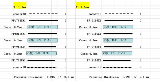
Stackup Documentation
The PCB fabrication drawing package includes detailed stackup documentation such as:
- Layer count, sequence and function – signal layers, plane layers etc.
- Dielectric materials used for each layer – FR4, polyimide etc.
- Conductive copper weight in ounces for each layer
- Signal trace widths, clearances and via styles used
- Panel sizes, finished board profile dimensions and tolerances
- Drill table for plated through holes and via hole sizes
- Netlist mapping traces to layers
- Rigid-flex stackup details if used
- Special notes on impedance control, back drilling etc.
Conclusion
The PCB stackup design defines the fundamental structure of the board and has a major impact on its electrical, thermal and mechanical performance. With increasing complexity and signal speeds, developing an optimal stackup has become a complex engineering task involving extensive modeling, simulation and analysis. Carefully planning the stackup configuration by managing tradeoffs between critical parameters is key to achieving a high performance, reliable and cost-effective multilayer PCB design.
Frequently Asked Questions
Q1. Why is stackup design important in multilayer PCBs?
The stackup impacts signal quality, EMI control, thermal management, manufacturability and reliability. Poor stackup design can lead to signal loss, cross-talk, reflection noise issues.
Q2. How many PCB layers are typically used?
4-6 layers are common for less complex boards. 8-16 layers used for more complex designs. High speed boards use 20+ layers.
Q3. What are split power and ground planes?
Split planes isolate different power domains and sensitive signals. For example, analog and digital circuits can have separate ground planes.
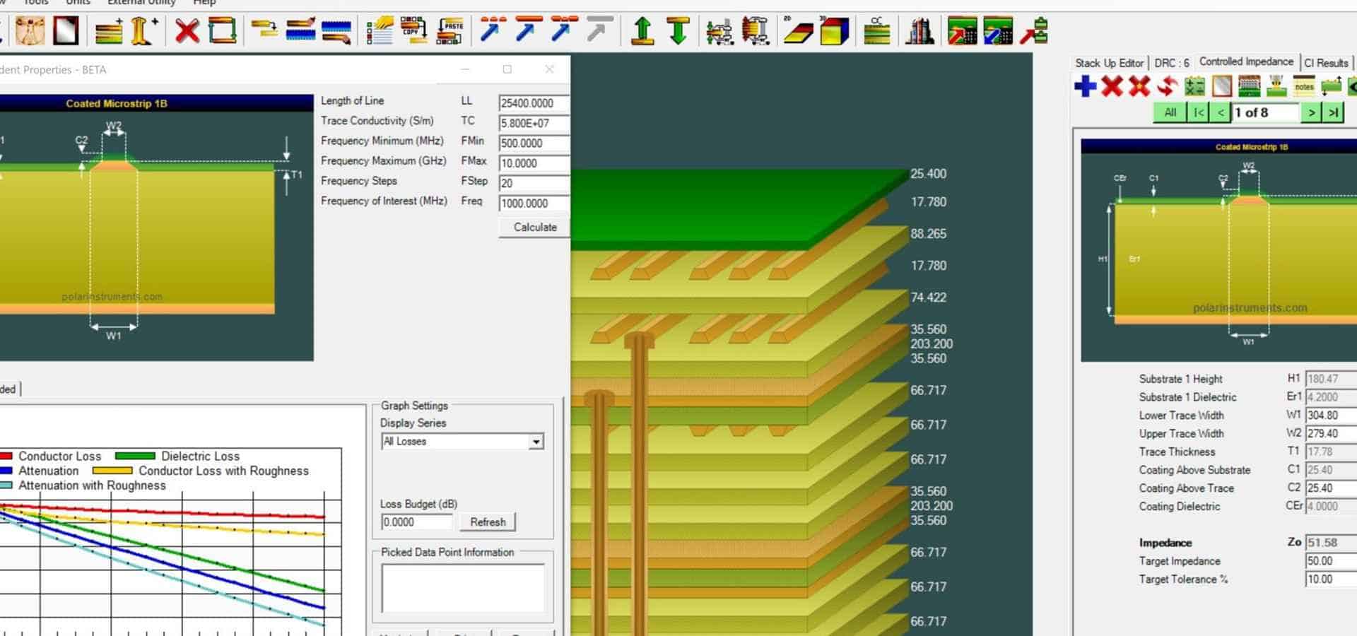
Q4. What is impedance control and why is it important?
Impedance control involves maintaining a constant controlled trace impedance through matching widths, spacing and dielectric materials. It prevents signal reflection losses.
Q5. Can flexible circuits be integrated with rigid PCBs?
Yes, combining rigid PCB sections with flexible circuits allows compact 3D routing. Careful analysis of the rigid-flex interface is required.


Leave a Reply