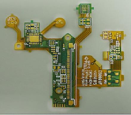
A PCB (printed circuit board) designer is a professional who specializes in the layout, routing and documentation of printed circuit boards using electronic design automation (EDA) software tools. They translate the logical electronic functionality envisioned by engineers into physical board constructions that serve as the foundation of electronic products and systems.
The role of a PCB designer involves a combination of engineering disciplines blending hardware, software and integration expertise focused specifically within electronics packaging domain specialization. Strong communication skills are also required to facilitate collaboration between electrical, mechanical and manufacturing engineering team members throughout a development program lifecycle.
Below is a more detailed overview exploring key aspects of what a PCB designer is, common job responsibilities, required skills, training options, career paths, and industry outlooks for this essential electronics industry occupation.
What Does a PCB Designer Do?
The primary work functions performed by a printed circuit board designer include:
Schematic Capture
- Interpret and translate electrical engineering schematics into logical connectivity models inside EDA tools
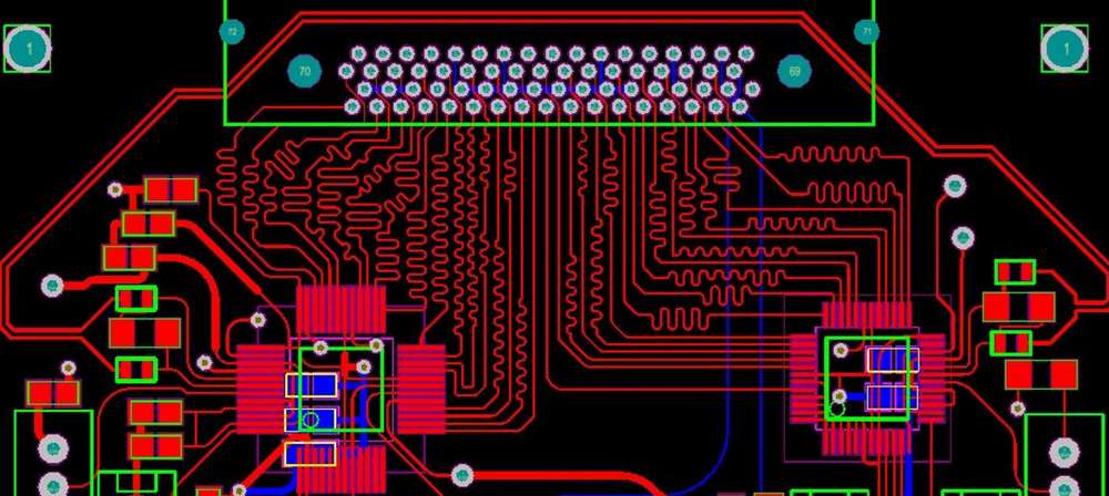
Board Layout
- Place components and route traces applying appropriate design rules and constraints
- Define layer stackups, hole sizes, trace widths, keepouts, etc to achieve manufacturability
Library Creation
- Generate device symbols and component footprints not available in existing libraries
Design Rule Checking
- Configure design rules for traces, vias, spacing, masks, plane connections, etc.
- Execute rule checks to validate compliance
Documentation
- Create manufacturing outputs – assembly drawings, fabrication prints, drill tables, etc.
- Annotate PCB artwork for identification and inspection
File Formats
- Import/export Altium, Cadence Allegro, Mentor, Zuken and other proprietary file types
- Manage versions across releases and changes
Product Data Management
- Enter metadata, change orders, life cycle status; integrate with PLM/ERP systems
Cost Analysis
- Estimate board fabrication and assembly expenses based on technology selections
Overall, PCB designers serve the vital role of translating ideas and specifications into physical layouts that can be reliably manufactured and assembled for prototyping, testing and production.
Key Technical PCB Design Skills
Successfully creating a functional printed circuit layout requires specific technical aptitudes and knowledge areas.
Electronics Fundamentals
- Read and apply information from basic schematics and block diagrams
- Understand common devices – ICs, transistors, resistors, capacitors, etc.
- Identify basic functions like amplifiers, power supplies, microcontrollers
- Apply Ohm’s law, voltage dividers, pull-up/pull-down networks
Hardware Skills
- Recognize standard connector types – USB, Ethernet, DVI
- Implement basic circuits – oscillators, filters, sensors, etc.
- Incorporate standard buses like I2C, SPI, UART
- Know implications of analog vs. digital systems
Design Practices
- Work within platform design constraints for performance, cost and schedule
- Apply appropriate derating factors and design margin philosophy
- Utilize design patterns like ground planes, decoupling, transmission lines
Software Tools
- Create schematics, layouts, generate manufacturing outputs
- Configure design rules, net classes, layer stacks
- Perform signal integrity analysis – AC, DC
- Thermal analysis – heat sinks, airflow, conduction
Manufacturing Integration
- Understand PCB fabrication processing limitations
- Accommodate automated assembly and test procedures
- Ensure quality and reliability requirements compliance
Documentation Standards
- Implement drawing notation symbols, callouts, annotations
- Generate drawings for fabrication, assembly, test
- Manage BOMs, component libraries, footprints
Supply Chain Logistics
- Source approved manufacturer components – AVLs
- Assign unique references designators and metadata
- Manage procurement cycles for quality and availability
Common PCB Designer Job Tasks
On a daily basis, printed circuit board designers work on a wide variety of tasks across multiple project lifecycle phases including:
Project Initiation Stage
- Attend project kickoffs to understand requirements, constraints, risks
- Study engineering block diagrams and external standard specifications
- Help assess technology readiness vs. solution space
- Estimate schedule efforts and cost projections
- Determine optimal design tool and library starting points
Logic Capture Phase
- Construct new schematics or import reference designs
- Enter engineering change orders (ECOs)
- Clean-up existing schematics if needed
- Define power schemes, grounding systems and interfaces
- Develop preliminary component placement plans
Physical Layout Stage
- Import floorplans, outline keepouts from mechanical CAD
- Place devices, route traces, assign plane polygons
- Author custom device symbols and land patterns
- Manage LVS checking and signoff reviews
- Document design outputs for fabrication and assembly
Qualification Testing
- Support prototype debugging by analyzing layout vs. actual hardware
- Recommend improvements for manufacturability or testability
- Implement engineering change orders as needed
Release to Production
- Finalize manufacturing Gerber and NC drill files
- Complete BOM, drawing packages and library revisions
- Archive design database and configuration files
Through this breadth of PCB design tasks, an individual designer may touch dozens of projects every year, interfacing with engineers across multiple disciplines.
PCB Designer Responsibilities
This demonstrates the breadth of ownership printed circuit board designers typically hold in developing, documenting and supporting electronics packaging solutions central to overall product success.
Desired Skills for PCB Designers
In additional to core layout competencies, here are some beneficial skills for versatile PCB designers:
Communication
- Convey ideas effectively through written reports, graphical visualizations and verbal discussions
Technical Writing
- Document procedures, sequence of operations, test plans
Time Management
- Prioritize activities based on schedules, resource availability and objectives
Creativity
- Approach challenges from different perspectives
Eye for Detail
- Identify subtle issues within complex system interactions
Teamplaying
- Cooperate across disciplines to determine optimal solutions
Leadership
- Guide more junior engineers by sharing knowledge
Adaptability
- Adjust to rapidly evolving tools, design methods and technology
Printed circuit board designers with excellent technical aptitudes paired with these auxiliary abilities offer tremendous value driving product development and sustaining engineering teams.
Education and Training for PCB Designers
While some junior PCB layout roles may only require vocational certificates or associate degrees, more advanced careers benefit from bachelor’s or master’s level engineering education paired with focused PCB tools training.
Undergraduate Degrees
Relevant undergraduate majors to gain foundational engineering knowledge include:
- Electrical Engineering
- Computer Engineering
- Electronics Engineering Technology
- Mechatronics
Coursework develops essential skills in areas like circuits, systems, controls, electronics, microcontrollers, instrumentation, and signals. Capstone projects provide early PCB exposure.
Graduate Degrees
For additional specialization in packaging interconnects, applicable graduate concentrations feature advanced programs in:
- Electrical Engineering – PCB Focus
- Electronics Manufacturing Engineering
- Electronics Materials Engineering
Studies provide sophistication in high density interconnections, characterization, fabrication processes, and industry focused best practices.
Vendor Software Tools
Major EDA tools vendors utilized at most PCB companies include:
- Altium Designer
- Cadence Allegro
- Mentor Xpedition
- Zuken CR-8000
Each platform has nuances. Formal training builds proficiency.
Continuing Education
Through conferences, publications and tutorials, ongoing learning expanding expertise across emerging standards, advanced tools techniques and novel technologies proves extremely beneficial over a long career.
By combining broad engineering fundamentals with targeted PCB technology specialties and applied software tool skills, aspiring designers can stands out when seeking that first role and better navigate increasing responsibility across decades in electronics.
PCB Designer Career Advancement Paths
Printed circuit board engineers have numerous options to progress their scope and impact over years of tenure through both individual contributor contributor and management oriented advancement paths.
Technologist Career Track
- Associate PCB Designer → PCB Designer → Senior PCB Designer → Principal PCB Designer
- Lead Designer → Chief Designer → Fellow
Management Career Track
- Section Leader → Department Manager → Director PCB Designers → VP Hardware Engineering
Dual Ladder Career Path
- Lead Designer → Principal Designer → Department Manager → Director → VP PCB Technology
ByKey enablers to navigate these typical designer career progressions include:
- Mastering additional EDA tools
- Expanding into related disciplines like signal integrity
- Developing specialized expertise in high complexity technologies
- Publication of papers and patents
- Increased leadership scopes and budgets
Those with long, successful tenure cultivate broad printed circuit board mastery spanning tools, fabrication, assembly, reliability, testing, layout techniques and team development. The valuable institutional knowledge retained from years of hard won experience creates engineers with very unique, differentiated capabilities to guide next generation technological innovations.
Global PCB Designer Job Market
Printed circuit board engineering stretches across geographic regions and industry verticals.
Salaries vary based on role seniority, specific industry, tools expertise, and degrees attained.
Global technology growth across nearly every industry continues driving demand for skilled printed circuit board engineers to transform ideas into physical electronic systems across consumer, networking, automotive, aerospace, medical, defense, IoT segments and more.
Outlook for PCB Design Careers
Printed circuit boards provide the central nervous system carrying power and signals across virtually all electronic devices. With exponential market growth predicted through 2030 as artificial intelligence, autonomous machines, edge computing, augmented reality, quantum devices and other innovations heavily rely on extremely sophisticated PCB advancements – the careers of those with expertise designing these electronics foundations hold strong through coming decades.
Industry analysts project >5% CAGR yearly growth for the global PCB market based on surging demand, with the following segments outpacing broader expansion:
- HDI/Microvia PCBs: 8-10% CAGR
- Flexible “rigid flex” circuit boards: > 15% CAGR
- PCBs for 5G infrastructure: 25%+ CAGR
These trends massively benefit designers knowledgeable in multilayer, high density interconnect, radio frequency and flexible PCB layout skill areas. Particularly PCB engineers who master complimentary analysis methods around signal and power integrity, thermal design and simulation fluency using advanced modeling tools stand to garner increased responsibility, compensation and career stability.
PCB Designer Job Frequently Asked Questions
What industries employ the most PCB layout designers?
The top industries hiring printed circuit board designers are:
- Consumer Electronics
- Networking & Telecommunications
- Automotive, Aerospace & Transportation
- Medical & Biotechnology
- Industrial Automation & Robotics
- Defense & Government Systems
What are typical entry-level PCB designer job titles?
Common entry points for new designers include PCB Designer Assistant, Associate PCB Designer, Junior PCB Designer, or Electronics Packaging Engineer. Internships also prime early training.
Is proficiency in ECAD software essential for PCB designers?
Absolutely – expertise navigating complex EDA tools like Altium, Cadence Allegro, Mentor Xpedition or Zuken CR-8000 is mandatory for schematic capture and board layout at nearly all companies. Open source options lag commercial maturity.
Can PCB designers work remotely?
Yes – remote and hybrid arrangements are common for most design functions using secure VPN access, managed file sharing platforms and real time video collaboration to enable productivity. Travel may be needed periodically for debugging labs, testing and releases.
What is the career outlook for printed circuit board designers?
Very strong as global electronics innovation heavily depends on PCB advancements. Market growth projections predict over 5% yearly expansion through 2030 across industries, with particular demand increases in multilayer boards, flex/rigids, RF designs, power electronics and rising density interconnects. Veteran designers are highly valued.
Conclusion
As electronic systems and enabling PCB technologies exponentially advance to integrate more functionality driving compute power, connectivity bandwidth and intelligence capabilities – the expertise to synthesize sophisticated printed circuit board packaging remains perpetually crucial. Companies with visionary products vitally depend on skilled PCB designers to translate ideas into physical layout innovations central to electronics breakthroughs. The career prospects for those mastering the interdisciplinary aptitudes bridging electrical engineering, software tools and manufacturing processes are therefore quite bright for decades to come across geographies as organizations compete to perfect amplifying technologies changing lives.


Leave a Reply