Introduction
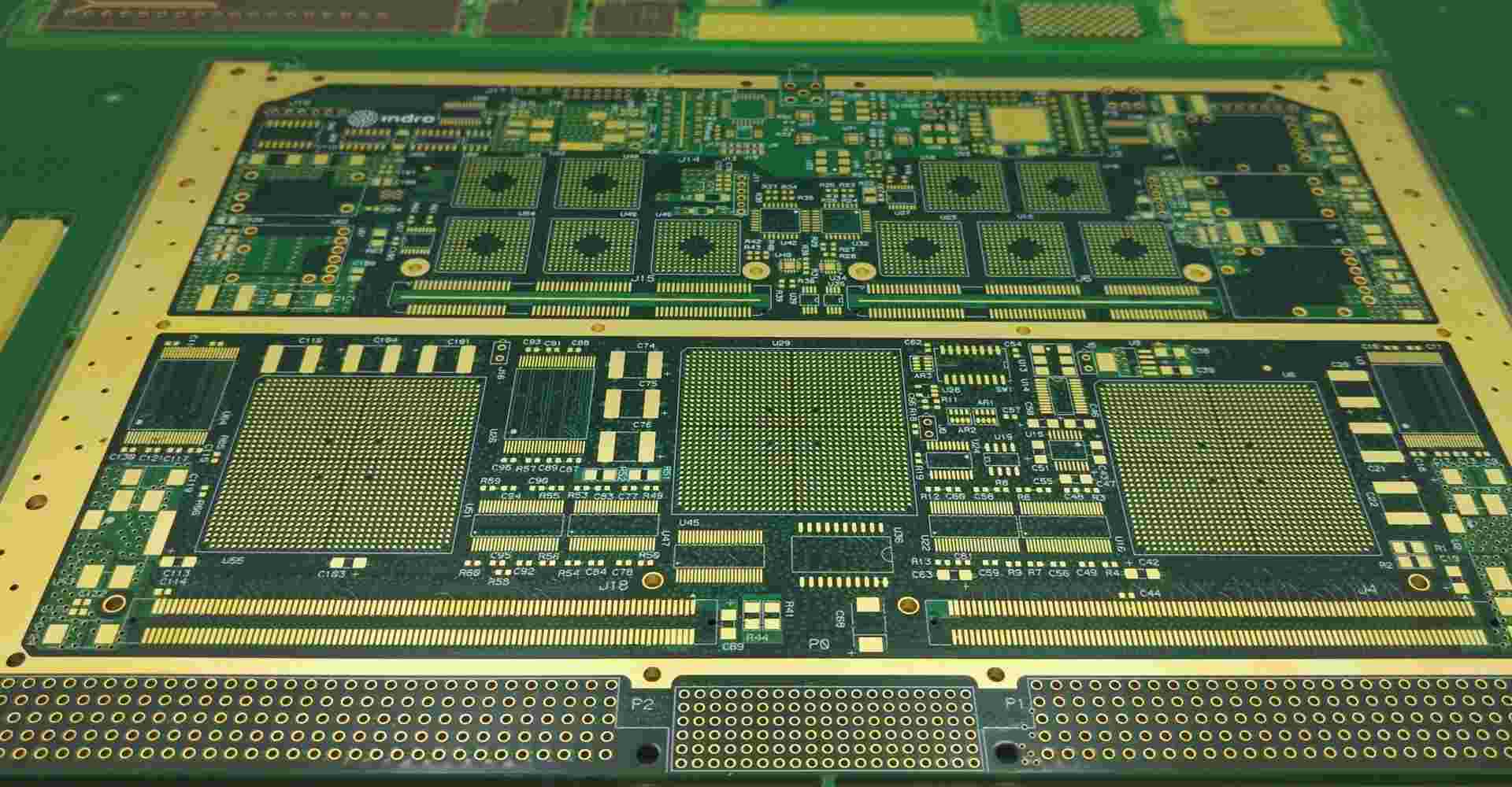
A multilayer printed circuit board (PCB) is a PCB made up of more than two conductive copper layers separated by dielectric material. Multilayer construction allows greater component density by routing connections between layers using vertical interconnects called vias. This enables more complex circuitry in less space compared to two-layer boards.
In a multilayer PCB, the layers are arranged in a sandwich structure. The outer layers are typically used for components and signals, while inner layers provide power delivery and ground planes. High density interconnects between layers are made possible by advanced fabrication processes.
Multilayer PCBs are widely used in advanced electronics to miniaturize complex devices like smartphones, computers, IoT gadgets, high-speed communications gear, and more. In this article, we’ll explore multilayer PCB basics, designs, applications, fabrication, and benefits.
Multilayer PCB Construction
A multilayer board is composed of alternating layers of rigid fiberglass reinforced dielectric substrate material and patterned copper foil. The core construction process steps are:
- Etch copper – Copper foil is laminated onto dielectric substrate sheets and circuit traces are etched using photolithography.
- Stack up layers – Alternating layers of etched dielectric and adhesive sheets (prepreg) are precisely aligned and laminated together under heat and pressure.
- Form vias – Holes are drilled through the stack and plated with copper to form vertical interconnects between layers.
- Finish – The edges and holes are trimmed. Surface finishes and coatings are applied.
The key technology enabling multilayer PCBs is the vertical interconnections or vias formed by high-precision drilling and copper plating. Let’s look further at vias.
Multilayer Vias
Vias provide electrical connections between different layers in multilayer PCBs. They consist of plated through holes passing vertically through the entire PCB stack. There are three main via types:
Through Vias
Through vias span all layers from the top to bottom of the stackup providing connectivity between the surface layers.
Blind Vias
Blind vias connect an internal layer to only one of the outer surface layers. This allows routing signals internally without using up surface space.
Buried Vias
Buried vias connect two or more internal layers without connecting to either surface layer. This keeps signals routed completely internally.
Vias allow routing connectivity independently on layers. High density, low resistance vias are essential for advanced multilayer boards with complex circuitry.
Typical Layer Stackup
While arrangements vary based on design needs, a typical layer stackup for a moderate complexity 4-layer PCB would be:
Layer 1 (Top):
- Primarily used for surface mount component pads and routing signal traces. May contain power and ground traces. Often a mixed signal layer.
Layer 2 (GND):
- Complete ground plane layer. Provides return paths for signals on Layer 1. Serves as ground reference.
Layer 3 (PWR):
- Power delivery plane. Distributes power from sources to components. Contains multiple power domains if needed.
Layer 4 (Bottom):
- Mirrors Layer 1, with component pads and signal routing. Components can be on one or both sides.
This arrangement intersperses power and ground planes between the signal layers, which:
- Isolates sensitive signals from noise.
- Minimizes ground loop areas.
- Reduces ground bounce and EMI.
- Allows controlled impedance signal routing.
Multilayer PCB Design
To effectively utilize the multilayer structure in a design, engineers must consider:
- Signal integrity – Controlled impedance traces, minimizing noise coupling between layers.
- Power delivery – Low impedance paths from sources to destination layers. Decoupling capacitors.
- Electromagnetic compatibility – Preventing emissions with ground planes. Managing inductive and capacitive coupling between layers.
- Thermal management – Heatsinking, thermal vias, and layer stacking for cooling.
- Manufacturing – Maintaining acceptable tolerances for registration, lamination, etc.
- Testability – Incorporating design for testability such as isolation, probing points, and boundary scan.
Multilayer design is an art mastered over years of training and experience. EDA tools help manage stackup complexity.
Multilayer PCB Fabrication
Producing multilayer boards requires advanced fabrication techniques:
- Alignment – Cutting edge laser alignment and lamination technology provide the tight (~25um) layer-to-layer registration needed.
- Drilling – High precision laser drills create small diameter (<0.2mm) vias with tight tolerances.
- Plating – Conductive vias with aspect ratios over 10:1 are plated using special chemistries.
- Lamination – Multi-stage lamination processes bond layers without leaving voids under high heat and pressure.
- Quality – Automated optical inspection (AOI) and x-ray are needed to ensure defect-free inner layer connections.
These processes push fabrication equipment to the limits. Only the largest shops can cost-effectively manufacture boards >16 layers at volume.
Multilayer PCB Applications
Some of the products that benefit from using multilayer PCB technology include:
- Smartphones – Complex multilayer boards crammed with components enable smartphone capabilities.
- Computers – CPUs, RAM, chipsets, and GPUs demand high-density multilayer boards for interconnections.
- Servers – High layer count boards with differential pair routing are used in servers for data centers.
- Automotive – ADAS, infotainment systems, and EV battery management rely on multilayer boards.
- Aerospace/Defense – Rugged multilayer designs withstand vibration in guidance systems and communications.
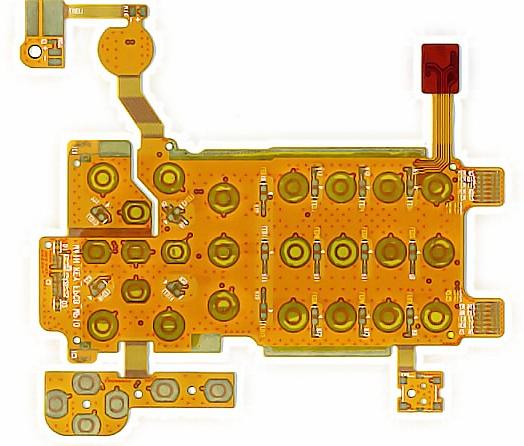
- Medical – Implants and instruments integrating sensors use flexible multilayer circuits.
Any application requiring advanced functionality in a compact form factor pushes designers towards multilayer implementations. As electronics evolve, multilayer PCBs become enabling technology.
Benefits of Multilayer Boards
What are the key benefits that make multilayer PCBs so ubiquitous in modern electronics?
- Increased density – More components and circuitry in a smaller footprint by going vertical.
- Miniaturization – Multilayer construction enables further device miniaturization and portability.
- Signal integrity – Careful layer stackup allows controlled impedance routing and isolation.
- High speed design – Termination, tuning, and matched lengths are possible with multilayer.
- Noise reduction – Ground planes shield sensitive signals layers from noise.
- Power distribution – Power and ground planes provide low impedance delivery.
- Thermal conduction – Inner layers conduct heat laterally to spread heat.
- Modularity – Different circuits can be routed on separate layers.
- Design security – Inner layers hide IP from reverse engineering.
- Reliability – Interconnections are buried inside the structure.
Without multilayer PCBs, the capabilities of modern electronic devices would not be possible.
Multilayer Challenges
Some of the key challenges in working with multilayer PCBs include:
- Design complexity – Routing, layer usage, and simulations get exponentially harder as layer count rises.
- Fabrication difficulty – High layer count boards push manufacturing capabilities. Thin dielectrics require tight process control.
- Testing difficulty – Limited physical access to intermediate layers makes inspection and troubleshooting hard.
- Tuning complexity – Achieving target impedance requires managing individual layer dielectric constants and weaves.
- Thermal issues – Inner layer heat spreading makes cooling analysis complex. Vias help transfer heat.
- Cost – Each additional layer increases fabrication cost. Advanced processes are required.
- Long lead times – Cycle times lengthen as layer count grows due to fabrication difficulties.
While certainly surmountable through good design, these factors limit applications of extremely high layer count boards. But the benefits outweigh challenges for most designs.
Future Outlook
Several trends point toward growing usage of multilayer PCB technology:
- Higher frequencies – Wider bandwidths demand careful attention to routing, tuning, and isolation best achieved with multilayer boards.
- Higher speeds – Supporting high speed serial buses like USB4 requires matched lengths only feasible on multilayer.
- Higher power – More power rails at lower voltages require interlaced power and ground planes.
- Higher pin counts – CPUs, FPGAs, and advanced packages have pin counts impossible to break out without multilayer boards.
- Miniaturization – Ever smaller and lighter devices continue to drive increased multilayer PCB utilization.
- Cost reduction – Improved drilling registration and lamination processing yields drive down fabrication costs, enabling more multilayer applications.
Multilayer PCBs will remain a key technology as electronics evolve and become further integrated into everyday devices.
Conclusion
Multilayer PCBs contain three or more conductive copper layers separated by dielectric substrate. This multilayer arrangement provides vertical interconnection capability through plated vias between the layers. Careful layer stackup design allows increased component density, improved electrical performance, reduced noise, and modularity. Multilayer construction is key to enabling the capabilities of smartphones, computers, communications gear, advanced automotive electronics, IoT devices, aerospace systems, and most leading edge electronics. Continued improvements in multilayer PCB fabrication technology will allow more layers, smaller features, and higher performance to meet demands as electronic applications continue advancing.
Frequently Asked Questions
Q1: What is the maximum number of layers possible in a PCB?
The practical limit today is around 30-32 layers, though experimental boards have been produced with over 50 layers. Extreme layer counts introduce fabrication challenges.
Q2: Can components be placed on inner PCB layers?
This is very rare. Some designs embed passive components like resistors and capacitors internally, but active ICs are almost always placed on the outer surfaces due to heat dissipation needs.
Q3: How are defects inside multilayer PCBs detected?
Automated optical inspection (AOI) checks outer layers. X-ray laminography is used to image internal features and detect voids or other buried defects.
Q4: What are some key differences between multilayer and double-sided PCBs?
Multilayers allow higher component density, power/ground planes, blind and buried vias, and greater modularization of design. But double-sided boards cost much less.
Q5: What are the main failure modes for multilayer PCBs?
Common failure causes include heat and vibration leading to trace or via cracks, electrochemical migration, and mechanical stress on plated through holes.


Leave a Reply