A flex PCB, also known as a flex circuit or flexible printed circuit board, is a type of printed circuit board (PCB) that is flexible and bendable. Flex PCBs consist of thin insulating polymer substrates like polyimide or polyester onto which conductive traces and components are mounted. They can bend, twist, and flex while still maintaining their electrical and mechanical connections. Flex PCBs are ideal for applications where flexibility, space savings, or movement is required.
Key Features of Flex PCBs
- Flexible – Can bend and flex repeatedly without damage
- Thin & lightweight – From 25um to 150um thick
- Durable – Withstands vibration, shock, and flexing
- Space saving – Fits into tight spaces and moving parts
- High reliability – Maintains connections despite movement
- Customizable – Can be shaped to fit unique form factors
Flex PCBs achieve their flexibility through the use of ultra-thin flexible dielectric substrates. Polyimide films like Kapton or Upilex are commonly used as the base material. Conductive copper traces are then etched or printed onto the flexible substrates. Components can be soldered directly to a flex PCB or connected using conductive adhesive or elastomeric connectors. The traces and substrate can bend and fold repeatedly without cracking or losing conductivity.
How are Flex PCBs Constructed?
Flex PCBs have a multi-layer laminated construction consisting of flexible dielectric substrates and conductive copper traces:
- Base Substrate – Thin polyimide film forms the flexible core of the PCB. This gives the board its flex and bendability. Standard thickness range from 25um to 150um.
- Conductive Layer – Very thin copper foil, typically 12um to 35um thick, is laminated onto the substrate. Photolithographic processes are used to etch the copper into circuit traces and pads.
- Coverlay – Additional polyimide dielectric layers are added on top of the conductive layer as coverlays and bondplies if the PCB has multiple circuit layers.
- Stiffeners – Optional rigid FR-4 stiffeners can be added in certain areas to facilitate component mounting.
- Overcoat – A thin polymeric solder mask coating protects the traces from environmental damage. Silkscreen legends can be printed for markings.
- Components – Passive and active components are soldered or adhesive mounted onto the flex PCB. Connectors can be added for mating with other PCBs.
The thin construction allows flex PCBs to deform, bend, twist, and fold repeatedly without damaging the conductors or substrate. The polyimide material provides excellent heat resistance as well.
Types of Flexible PCBs
There are several common types and constructions of flexible PCBs, including:
Single Layer Flex Circuits
- Consist of a single polyimide substrate layer and one layer of copper traces
- Lowest cost option
- Typically used for simple interconnection circuits
Double Layer Flex Circuits
- Consist of two copper circuit layers bonded together by an adhesive dielectric layer
- Provides higher circuit density with traces on both sides
- More common construction type
Multilayer Flex Circuits
- Have 3 or more conductive copper layers separated by polyimide dielectric bond ply layers
- Allows for complex, high density circuit designs
- Used for advanced rigid-flex applications
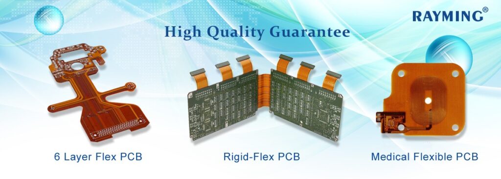
Rigid-Flex PCBs
- Combines rigid FR-4 PCB sections with flexible polyimide sections
- Rigid sections provide stability for mounting components
- Flexible sections allow dynamic movement and bending
In terms of protective coatings, flex PCBs are typically covered on one or both sides by a thin solder mask for insulation and mechanical protection. They can also have stiffeners, shields, or covers applied in certain areas.
Typical Applications of Flex PCBs
Some common products, components, and applications that utilize flexible PCB technology include:
- Wearable devices – watches, fitness trackers, health monitors
- Medical devices – hearing aids, implants, monitors
- Consumer electronics – cellphones, cameras, display screens
- Automotive – sensors, control units, antennas
- Robotics – arms and joints, sensors
- Aerospace – control surfaces, antennas
- Instrumentation – sensors, probes
- Missiles & weapons systems – guidance systems
- Industrial – pan/tilt camera modules, automation
Flex PCBs are well suited for these applications due to their tight space requirements, motion needs, or rugged conditions. The dynamic flexing also helps reduce wiring and improves reliability compared to discrete wiring harnesses.
Benefits and Advantages of Using Flex PCBs
There are many important benefits that make flexible PCBs advantageous versus rigid PCBs for certain applications:
- Flexible – Can be bent, folded, twisted dynamically
- Thin, lightweight – Takes up less space, lower mass
- Durable – Withstands vibration, shock, and repeated flexing
- Higher reliability – Flexible construction withstands movement
- Complex shapes – Can be folded into 3D configurations
- Space savings – Conforms tightly to enclosed spaces
- Simplifies assembly – Integrates interconnections into one component
- Heat dissipation – Polyimide withstands higher temps
- RF transparency – Allows signals like antennas to transmit through the PCB
By taking advantage of these benefits, flex PCBs can often simplify designs, improve reliability, save space, reduce assembly steps, and lower overall system weight versus traditional rigid PCB solutions. The trend towards smaller, higher performance portable electronics continues to drive increased adoption of flex circuits where flexibility is required.
Design Considerations for Flex PCBs

Engineers should keep several important design guidelines in mind when working with flexible PCBs:
- Bend radius – Avoid tight folds, build in generous bend radius (>10X substrate thickness)
- Creasing – Prevent creasing which can damage conductors
- Rigid sections – Allow for islands or windows of rigid PCB sections for mounting components
- Layer stackup – Stackup arrangement impacts flexibility – keep rigid layers towards middle
- Conductor width – Keep traces wide (>0.15mm) to survive flexing without cracks
- Adhesives – Use flexible, high elongation adhesives qualified for dynamic bending
- Vias – Use staggered pad or tented vias to relieve stress concentrations
- Reinforcement – Consider reinforcing high flex areas with stiffeners
- ESD protection – Use proper ESD grounding, handling, and protection
- Testing – Test PCB flex cycles, lifetime expectancy
Paying attention to these guidelines helps ensure reliable performance of the circuits over the product lifetime. Flex PCB layouts require specialized design expertise.
Flex PCB Materials
Selecting the right materials is key to designing durable, reliable flexible PCBs. Here are some of the typical materials used:
Substrate Films:
- Polyimide (Kapton, Upilex) – most common flexible dielectric
- Polyester (PET) – lower cost but lower temp tolerance
- PEEK, Polyimide-amide – high temp applications
Bonding Adhesives:
- Acrylic
- Modified epoxy
- Polyimide
Conductor:
- Copper – rolled annealed, electrodeposited or sputtered
Coverlay:
- Liquid photoimageable (LPI) solder mask
- Ink-coated dielectric films
Stiffeners:
- FR-4 glass epoxy laminates
- Aluminum
- Stainless steel
Polyimide films like Kapton provide the best combination of flexibility, dimensional stability, and high temperature resistance. IPC standards define the qualifications for base materials and bondply adhesives used in flex PCB designs.
Fabricating Flexible PCBs
There are a variety of methods used to fabricate flex PCBs:
- Photolithography – Conventional PCB lithographic processing of Laminate-Image-Develop-Etch-Strip
- Printed electronics – Uses conductive and insulating inks printed in patterns
- Laser direct structuring – Laser activates substrate so copper will deposit onto activated areas
- Laser ablation – Removing copper with a laser
- Metal etching – Subtractive etching of metal foils using chemicals
Once the conductors are patterned, components can be assembled by:
- Soldering – Reflow or hand soldering
- Conductive adhesive – Epoxy with silver or nickel filler
- Thermosonic bonding – Ultrasonic pressure bonds gold wire to gold plated pads
Photolithographic processing is the most precise and common method used to produce commercial flex PCBs. The thin material demands specialized processing considerations versus rigid boards.
Flex PCB vs Rigid PCBs
While rigid PCBs still dominate electronics, flex PCBs offer advantages in certain applications:
| Parameter | Flex PCB | Rigid PCB |
|---|---|---|
| Flexibility | Yes | No |
| Thickness | 25 – 150 μm | 0.6 – 1.6 mm |
| Weight | Light | Heavier |
| Layer Count | 1- 12 layers | Up to 30+ layers |
| Bend Radius | Tight bends possible | Limited bendability |
| Reliability | High flex life | Brittle, cracks under flexing |
| Temp Range | -55°C to 150°C | -55°C to 130°C |
| Applications | Dynamic, tight spaces | Stable, rigid mounting |
| Cost | Higher | Lower |
So in applications requiring thinness, tight space, flexibility, or dynamic bending, flex PCBs provide the necessary properties over rigid technology. The tradeoffs are higher cost and typically lower layer counts versus rigid boards.
Flex PCB Cost Factors
Several factors impact the costs of flex PCBs:
- Number of conductive layers – More layers increases cost
- Board size – Manufacturing panels have fixed sizes, so smaller boards are less efficient
- Flex vs rigid areas – Flexible material is more expensive than rigid sections
- Tolerances and features – Tighter tolerances require more processes
- Volume – Higher quantities means lower cost per board
- Special processes – Additional steps like via tenting or gold plating adds cost
In general, flex PCBs range from being 2-5 times as expensive as an equivalent rigid PCB. But the benefits flex PCBs provide including flexibility, durability, and assembly consolidation often justify the premium cost.
Future Trends for Flexible PCBs
Some trends shaping the future of flex PCB technology include:
- Thinner flexible substrates – Enables smaller and lighter electronics
- Advances in printed electronics – Printed conductors and circuits, eliminates etching
- Stretchable flex circuits – Flexible components that can stretch as well as bend
- Wearable technology – Flex circuits ideal for wearable health and fitness devices
- Flexible displays – Flexible OLED displays relying on flex interconnects
- Environmental resistance – Improved flex materials to withstand harsh conditions
- Higher density traces – Finer lines and spaces, high layer count boards
- IoT devices – Flexible sensor nodes for smart city and home applications
Continued innovation in flexible PCB materials, fabrication methods, and design tools will allow flex circuits to enable future generations of thin, lightweight, and reliable electronics.
Flex PCB Design Guidelines
Here are some key guidelines to follow when designing a flex PCB:
- Minimize component placement in high-flex areas to avoid damage from repeated bending
- Use large bend radii – minimum 10X the flex layer thickness for dynamic bending, 5X for static bends
- Stagger placement of components on either side of centerline to balance stresses
- Avoid sharp 90° bends – use rounded curves instead
- Plan for adhesive-free zones to concentrate flexing in those areas
- Eliminate creasing which can damage conductors
- Widen traces (> 0.15mm) in flex areas since copper fractures easier
- Use robust, flexible component attachment methods like adhesive bonding
- Include test points to verify electrical continuity during prototyping flex cycles
- Perform fatigue life testing to validate flex design requirements
- Cover conductors with solder mask for insulation and mechanical protection
- Ensure complete encapsulation around pad openings to prevent copper wicking
- Select flexible, high elongation adhesives to withstand repeated bending
Following these guidelines helps avoid common failures like cracked conductors, delamination, pad lifting, and broken connections. Consult with an experienced flex PCB manufacturer during the design process to ensure manufacturability and reliability. Careful design is necessary to benefit from the advantages of flex circuits.
Frequently Asked Questions
Here are some common questions about flex PCBs:
Q: How many times can a flex PCB be bent before failing?
A: A well-designed flex PCB can withstand hundreds of thousands of dynamic flex cycles. Factors like bend radius, conductor width, and materials impact flex life. Testing is used to validate cycles.
Q: Can components be mounted on flex PCBs?
A: Yes, components can be surface mounted or through-hole mounted. Adhesives or elastic connectors are often used. Rigid sections can also be incorporated.
Q: Are flex PCBs expensive to produce?
A: Flex PCBs typically cost more than rigid PCBs, often 2-5X as much, due to specialized materials and processes. But they can reduce wiring and assembly costs.
Q: What are some differences from rigid PCB fabrication?
A: Flex PCBs require thinner metal foils, specialized substrates, flexible component attachment methods, and handling considerations versus standard rigid PCBs.
Q: How small can flex PCB traces and spaces be?
A: Typical flex PCB lines and spaces can be as small as 100 μm (4 mils), although larger traces are used in dynamic bending areas.


Leave a Reply