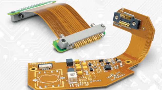
Printed circuit boards (PCBs) are essential components in virtually all modern electronics. They provide the mechanical structure and electrical connections between components that enable electronic devices to function. An important aspect of PCB design and manufacturing is testing, both to ensure proper functioning during production and to diagnose issues during product use. This is where test points on the PCB play a crucial role.
Test points, also known as test pads or probe points, are conductive areas on a PCB that allow reliable access to signals and components for testing purposes. They allow engineers to accurately probe circuits and nodes to verify that the PCB is working as intended. Understanding the different types of test points, their functions, design considerations and best practices is key knowledge for PCB designers and test engineers.
This article provides a comprehensive overview of PCB test points, looking at the different categories, applications, design guidelines and more. We’ll cover key questions like:
- What are the main types of test points and their purposes?
- Where are test points located on a PCB?
- What are important test point design considerations?
- How is testing performed using test points?
- What standards and best practices apply to test points?
Gaining a solid understanding of PCB test points will equip you with knowledge to implement robust testing while optimizing your board’s design and manufacturability.
Types of Test Points
There are several types of test points that serve different testing needs:
Test Pads
- Circular or oval conductors for probe contact
- Provide access to test nodes, traces, vias, components
- Various sizes to accommodate probe tips
Test Pins
- Tall metal pins extend above board surface
- Allow secure grasp of probes for stability
- Better access when board is crowded
Vias
- Plated through-holes connecting layers
- Double as test points for inner layer access
- Microvias also useful to route signals to top layer
Castellated Holes
- Plated half-holes along board edge
- Probe points for testing after fragmentation
- No need to dedicate board area for test pads
Test Coupons
- Dedicated conductor shapes to test trace integrity
- Verify quality of fabrication process like plating
- Include coupons for adhesion, resistance, spacing
Embedded Components
- Test components like switches, LEDs, etc.
- Facilitate testing of circuits/ Signals
- May be temporary or permanent
Boundary Scan Pads
- Standardized pads for boundary scan testing
- Adhere to specifications like JTAG
- Facilitate automated circuit testing
Programming/Debug Headers
- Interfaces for device programming and debugging
- Often dual-purpose as test points
- E.g. JTAG, SWD, ICSP headers
This covers the primary types of test points leveraged on PCBs during the design, fabrication, assembly and testing processes. Next we’ll look at where test points are physically located on the board layout.
Test Point Locations on PCBs
Carefully planning where to place test points allows efficient access during testing. Here are common PCB locations for test points:
Near components – Points adjacent to chips/modules to probe signals or test connections.
Near connectors/headers – Test interface pins and signals entering/exiting the PCB.
Near planes – Access points for checking power/ground planes.
Circuit nodes – Test points routed to internal circuit nodes needing verification.
Board edges – Castellated holes along edges for fragmentation testing.
Corner markings – Identifiers screen-printed in corner areas away from circuits.
Test regions – Dedicated board area with dense test points not assembled.
Temporary points – Added only for initial engineering testing, not production.
Programming headers – Standardized headers like JTAG used for programming and testing.
Boundary scan – Pads connected to boundary scan path to facilitate automated testing.
Strategically placing test points in these areas provides access while minimizing impact on the PCB layout.
Test Point Design Considerations
Several important factors to consider when designing test points:
Size – The pad size must match the probes used for testing. Too small risks open circuits, while too large takes up space.
Spacing – Adequate spacing between test points prevents accidental shorting when probing.
Routing – Accessible routing to test nodes, minimizing vias and stubs. Avoid crossing unrelated traces.
Labels – Clear labels or markings indicate the associated component/node being probed.
Impedance – Test points should not alter characteristic impedance of matched transmission lines.
Layers – Often placed on outer layers, but inner layer access points are also necessary.
Removal – Temporary test points only used in engineering can be mechanically removed.
Interference – Keep high frequency test points separated from noisy digital traces.
Testability – Virtual probes and boundary scan access must also be considered for automated testing.
Taking these factors into account results in test points that provide robust, convenient access while maintaining signal and board integrity.
Performing Testing
There are several techniques to actually test circuits using the various types of test points:
Manual probing – Using handheld probes with oscilloscopes, DMMs and specialized probing equipment.
Flying probes – Automated probes on fixtures target exposed test pads across the board.
Bed of nails – Board pressed onto a fixture with spring-loaded probes aligned to test points.
Boundary scan – Specialized probes target JTAG/boundary scan pads for standardized testing.
Built-in instrumentation – Onboard chips with debug/test modes accessed via headers.
Embedded test – Circuits like embedded LEDs, switches and instrumentation to facilitate testing.
Power polling – Check continuity by sequentially powering board sections to identify faults.
In-circuit test – Individual components tested dynamically while powered up on board.
Having accessible and well-designed test points enables the use of these techniques to thoroughly validate PCB operation.
Standards and Best Practices
Certain standards and guidelines are worth following when implementing test points:
- IPC-2221 – Defines various types of test pads, dimensions, layout and characteristics.
- IPC-A-610 – Acceptability standards for attributes like pad finish, spacing, labeling.
- IEEE 1149.1 – JTAG boundary scan pinouts and protocols.
- IEEE 1149.7 – Compact JTAG connectors reducing test pads.
- SWD – Cortex debug headers for ARM processor debugging/testing.
- Labels – Use universally recognized labels like L1, TP5 vs ambiguous text.
- Locations – Group test points together when possible versus scattering them.
- Temporary points – Make temporary test points visually distinguishable from permanent ones.
- Impedance – Match test points to trace impedance to avoid reflections.
Adhering to standards maximizes the utility of test points for debug and diagnosis while minimizing negative impacts on the PCB layout and signal integrity.
Advantages of Test Points
Implementing appropriate test points on a PCB provides several benefits:
- Enable thorough testing and troubleshooting to confirm proper PCB functioning.
- Allow engineers to validate performance at each stage from design through production.
- Facilitate debugging and repair by providing internal node access that diagnostics can leverage.
- Reduce dependence on internal instrumentation like built-in self-test for validation.
- Provide controllability and observability needed for conformance testing to requirements.
- Test points used across manufacturing reduce capital costs of bed-of-nails fixtures.
- Support testing automation through standardized interfaces.
- Temporary test points assist prototyping and new product introduction prior to high-volume production.
In summary, test points are indispensable enablers of PCB testing methodologies that are necessary to ensure reliability and performance.
Conclusion
Test points in various standardized forms are integral parts of printed circuit board design to facilitate validation, troubleshooting and repair throughout the electronics lifecycle. The key test point types provide access to signals at component pins, connectors, vias, hidden layers and circuits nodes based on thoughtful design considerations. Strategically placed test points following accepted guidelines allows engineers to thoroughly probe and debug boards using manual and automated techniques. As PCBs grow more complex, test points will become increasingly important for verification and diagnostics. electronics engineers equipped with knowledge of their purposes, design and utilities will produce robust boards ready for efficient testing.
Frequently Asked Questions
Q: Why are some test points connected to ground or power planes?
A: It is common practice to route some test points to ground or power planes as reference points during debugging. Probing these ensures a steady voltage baseline when measuring at other circuit nodes. It also helps identify shorts or open circuits related to ground/power.
Q: Can test points impact signal or power integrity?
A: Poorly designed test points can introduce issues like reflections, crosstalk, stubs and added capacitance that degrade signal and power integrity. Well-designed test points following layout best practices will not significantly influence performance. Strategies like matching trace impedances can mitigate issues.
Q: How can testability be improved when debugging boards?
A: Steps to improve debuggability include adding test points to internal nodes, ensuring boundary scan coverage, incorporating programming headers for access to onboard instrumentation, implementing built-in self-tests, and labeling test points clearly.
Q: Should test points be added to production PCBs?
A: Test points required for production testing or field diagnostics should remain on production boards. But temporary test points only needed in engineering prototypes can be mechanically removed from production boards to reduce costs if they are distinguishable.
Q: What are flying probe testers used for?
A: Flying probe testers use automated probes to contact exposed test points and rapidly validate electrical connectivity, continuity or isolation across a complete PCB. This assists with detecting assembly defects and avoiding dedicated test fixtures.


Leave a Reply