Printed circuit boards (PCBs) provide the foundation for electronics packaging and component assembly. PCB thickness is a critical design parameter impacting manufacturing capabilities, utilization, and reliability. Selecting suitable laminate thicknesses requires understanding industry conventions, constraints, and use case tradeoffs.
This article explores common PCB substrate thicknesses across typical applications along with selection criteria.
Overview of PCB Thickness Ranges
Circuit board thicknesses span a wide spectrum from flexible films less than 0.1mm thin to rigid laminates over 5mm thick. Material stacks comprising dielectric and conductive layers have viable thicknesses suited for particular applications.
Thin PCBs
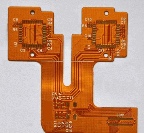
Thin printed boards utilize dielectric films allowing tight rollable packages ideal for space constrained flexible circuits. Thin laminate construction facilitates advanced stacking techniques like folded flex assemblies.
Common thin PCB thicknesses range from:**
- 0.025mm – 0.050mm (1mil – 2mil)
- 0.051mm – 0.100mm (2mil – 4mil)
Standard Thickness PCBs
The majority of rigid laminates used for typical PCB designs have substrate thicknesses between 0.8mm to 2.0mm. Component density and layer counts determine suitable thicknesses balancing stiffness, manufacturability, and reliability.
Typical standard thickness boards span from:
- 0.5mm to 1.2mm (20mil – 48mil)
- 1.6mm to 2.0mm (63mil – 78mil)
Thick PCB Boards
Applications requiring high currents or power levels utilize thicker dielectric substrates over 2.5mm providing necessary insulation properties. Thick metal backing planes help manage temperatures.
Common thicker boards used for power electronics or high frequency RF designs range from:
- 2.5mm to 3.2mm (100mil – 125mil)
- 4.0mm to 5.0mm (160mil – 200mil)
PCB Substrate Thickness Ranges
| Category | Thickness Range |
|---|---|
| Thin Boards | 0.025mm – 0.100mm |
| Standard Boards | 0.5mm – 2.0mm |
| Thick Boards | 2.5mm – 5.0mm |
Key Factors Influencing PCB Thickness
Determining appropriate printed circuit board thicknesses depends on several interrelated design elements including:
Circuit Density
Board thickness impacts component spacing and routing capabilities. Thinner laminates facilitate dense component mounting with tight pitch assemblies and high density interconnected (HDI) techniques. Consumer products like phones utilize 0.4mm – 0.8mm boards allowing smashed signal and power routing between BGAs. In contrast, simple microcontroller boards may exploit 1.6mm substrates.
Layer Count
Multilayer boards sandwich dielectric cores between conductive copper foils. Manufacturer capabilities balance layer counts,AspectRatio Ratios (AR), and thicknesses. Thin multilayers typically utilize 3-8 layers while standard designs exploit 10-36 layers using thicker cores maintaining sufficient rigidity.
Currents and Temperatures
Applications demanding higher currents generate thermal loads requiring management. Thicker metal cores or backing planes combined with thicker dielectrics suits these power boards better allowing sufficient insulation while conducting heat laterally out layers instead of through laminates.
Frequency and Losses
Electrical design properties like dielectric loss tangent and impedance change with frequency and material thickness impacting performance. Controlled laminate thickness combined with right dielectric materials essential for high frequency analog and RF boards above 500MHz minimizing losses.
Stiffness and Handling
Thin flexible boards unable to independently support components may require bonding to rigid frames during assembly preventing warpage increasing manufacturability. However thicker standard boards over 1.0mm provide suitable stiffness facilitating processing while avoiding breakage.
Key Drivers of Printed Circuit Board Thicknesses
| Driver | Criteria |
|---|---|
| Circuit Density | Component clearances, HDI stacking |
| Layer Count | Dielectric and foil build up |
| Currents | Thermal loads and insulation needs |
| Frequency | Impedance control and loss effects |
| Stiffness | Robustness for handling and assembly |
Accounting for all factors allows determining viable PCB thicknesses for specific applications.
Popular Dielectric Materials by Thickness
Various insulating substrate materials used for printed circuit board fabrication have common thickness conventions driven by chemical families, reinforced composites, and intended applications.
FR-4 Thicknesses
Flame retardant FR-4 glass reinforced epoxy laminates represent the most prevalent PCB substrate used for majority of commercial circuits from consumer electronics to industrial controls.
Typical FR-4 thickness grades include:
- 0.4mm (16 mil)
- 0.8mm (31mil)
- 1.0mm (40mil)
- 1.6mm (63mil)
- 2.0mm (78mil)
Selecting suitable FR-4 thickness depends on number of foils, target impedance, panel utilization, and handling needs.
High Frequency PCB Materials
Performance sensitive radio frequency (RF) and high speed digital logic boards utilize advanced dielectric materials engineered for tighter property control, dimensional stability, lower losses, and smooth copper surfaces.
Regular high frequency laminate thicknesses span:
- 0.5mm (20mil)
- 0.8mm (31mil)
- 1.6mm (63mil)
Qualifying appropriate material thickness provides sufficient rigidity while meeting electrical impedance needs.
Metal Core & Metal Backed PCBs
Metal core printed circuit boards (MCPCB) utilize an internal aluminum or copper heat spreader foil to conduct heat laterally out of the center laminates. This enables managing thermal rise from high power components.
Typical metal core PCB thickness grades include:
- 1.0mm (39mil)
- 1.6mm (63mil)
- 2.0mm (78mil)
- 3.0mm (118mil)
Likewise, metal backed boards use thicker external foil layers as heat sinks which can be selectively thermally connected to inner planes by plated through holes.
Printed Circuit Board Size and Thickness Interactions
Determining viable laminate thicknesses requires accounting for panel dimensions and target PCB size to enable efficient panel utilization, processing yields, and mechanical capabilities.
| Panel Size | Typical Thickness Range |
|---|---|
| 18″ x 24″ | 0.4mm – 3.2mm |
| 21″ x 24″ | 0.8mm – 4.2mm |
| 24″ x 18″ | 1.0mm – 6.0mm |
| 24″ x 36″ | 1.6mm – 6.0mm |
Larger panels support thicker boards however process capabilities often dictate substrate sizes. Consumer goods extensively adopt 18″ x 24″ panels for cost efficiency. Medical products frequently use smaller 21″ x 24″ sizes meeting tighter tolerances.
Standard Thickness Boards By Application
Printed circuit board thickness conventions also exist across applications and industry verticals correlated to manufacturing capabilities, assembly technologies, reliability needs, and design complexity.
Consumer Electronics
- Portable devices: 0.4mm – 0.8mm
- Appliances: 0.8mm – 1.6mm
Automotive Electronics
- Control units: 1.0mm – 1.6mm
- Power modules: 2.5mm+
Industrial & Instrumentation
- Sensors/transmitters: 1.6mm
- Motor drives: 2.4mm – 3.2mm
Computers & Servers
- Motherboards: 0.8mm – 1.6mm
- Backplanes/RISers: 1.6mm – 2.5mm
Medical Equipment
- Instruments & Diagnostics: 1.6mm
- Patient monitors: 2 layers 0.8mm / 4+ layers 1.6mm
Aerospace & Defense
- Avionics controls: 1.6mm – 2.5mm
- Radars: 3.2mm+
Standard thickness conventions maximize manufacturing utilization and availability. However new applications may justify qualifying alternative thicknesses on existing production lines by correlating suitable panel sizes.
Considerations When Selecting PCB Thicknesses
Balancing numerous interdependent factors allows determining viable laminate thicknesses matching performance needs, technology capabilities, and product goals.
Key considerations include:
- Density of components and routing
- Layer counts and aspect ratios
- Operating temperatures and power
- Impedance control needs
- Manufacturing yields
- Integrity for environmental stresses
- System assembly clearances
- Correlating thickness with panel sizes
Analyzing critical drivers against target applications helps qualify ideal PCB thicknesses. Useful techniques involve building evaluation boards at different thicknesses measuring key parameters or thermal cycling samples assessing robustness.
Simultaneously considering electrical, mechanical, thermal, and assembly requirements allows optimizing printed circuit board thickness.
Trending Toward Thinner More Advanced Boards
Continual technology advances allow condensing higher densities of components onto increasingly compact printed circuit boards. The sustained trend pushes toward thinner laminates with more layers as enabled by emerging manufacturing capabilities.
Denser Component Assembly
Tighter component packaging such as wafer level scale integrated circuits and advanced QFN assemblies allow mounting over 1,500 parts per square meter pushing line widths under 100 microns. This explosion in density impossible without thinner laminate fabrication.
HDI Build Up Layers
High density interconnect construction techniques facilitate complex layer stacks exceeding 30 total buildup layers allowing embedding actives and passives. HDI depends on thinner cores or substrates while accumulating more thin exterior foil layers.
Improved Registration Accuracy
Tighter process controls with advanced digital imaging allows holding tighter layer-to-layer alignments under 50 microns. This permits reducing substrate thicknesses which previously provided margins absorbing registration errors during fabrication.
Enhanced Roughness Tolerances
Smoother laminate materials with 5 microns or less copper surface roughness reduces electrical losses at higher frequencies necessary for impedance control up to 50+ GHz. Thin substrates aid in achieving necessary RF stack ups.
PCB Thickness Guidelines By Application
The below guidelines provide general printed circuit board thickness ranges correlated to common applications as a starting point when making thickness selections. However unique criteria may justify deviations when accounted for during design qualification.
| PCB Application | Recommended Thickness Range |
|---|---|
| Wearables/Internet-of-Things | 0.4mm to 0.8mm |
| Handheld/Portable Devices | 0.5mm to 1.0mm |
| Automotive Body Modules | 1.0mm to 1.6mm |
| Industrial Instrumentation | 1.6mm to 2.0mm |
| Servers/Data Networking | 0.8mm to 1.6mm |
| LED Lighting Drivers | 1.6mm to 2.5mm |
| Electric Vehicle Powertrain | 2.5mm to 5mm |
| cellular Infrastructure | 2mm to 3mm |
| Aerospace/Defense Avionics | 1.6mm to 3.2mm |
Use these thickness guidelines as starting points then refine based on specific requirements.
Conclusion – Choosing Suitable PCB Thicknesses
Printed circuit board thickness directly influences routing densities, layer stacks, electrical performance, manufacturability, and reliability making it an essential design parameter requiring thorough analysis.
New product development should begin considering preliminary board thicknesses based on industry conventions and guidelines then refine selections by analyzing interrelated assembly, production, and operating requirements against target applications.
Carefully qualifying PCB laminate thicknesses provides the foundation enabling optimized electronics packaging, faciliting efficient manufacturing, and ensuring reliable products.
Frequently Asked Questions
Q: How thick of a PCB is needed for high power LEDs?
A: High brightness LEDs can generate significant thermal loads requiring metal core PCB (MCPCB) constructions typically 2.5mm to 5.0mm thick. The thick metal heat spreader layer laterally dissipates heat from dense LED arrays while thick dielectric insulation prevents shorts.
Q: What PCB thickness is easiest to hand solder?
A: Standard 1.6mm thick boards provide suitable mass to prevent warping during hand soldering operations. Thinner 0.8mm PCBs risk slight bending complicating soldering or requiring additional support like carrier plates. Components lead formations also correlate with thickness.
Q: What Determines PCB thickness for multiple layers?
A: Closely correlating board thickness with total layer counts ensures maintaining suitable aspect ratios under 10:1 for processing yields. This often drives adopting thicker 1.6mm – 2.0mm boards when exceeding 12 circuit layers. Panel size interactions also influence thicknesses.
Q: How do material costs compare across PCB thicknesses?
A: Printed circuit board raw material cost generally correlates directly with thickness. Double-sided 0.8mm FR-4 boards can run around $10 per square foot while 4-layer 2.5mm laminates approach $50. Even greater thickness variation exists on more exotic materials like PTFE or ceramic substrates.
Q: Why use thinner PCBs for mobile consumer electronics?
A: Thinner laminate materials allow mounting ICs and components in tighter pitches facilitating smashed routing for denser layouts. This enables condensing more functionality within compact form factors while maintaining suitable flexibility resisting cracking. Typical smartphones adopt 0.4mm to 0.8mm PCBs.


Leave a Reply