Introduction to Wave Soldering
Wave soldering is a large-scale soldering process used for efficiently soldering electronic components to printed circuit boards (PCBs). It is the most common mass soldering method used in the electronics manufacturing industry, thanks to its ability to quickly and reliably solder through-hole components. In this comprehensive article, we will explore the fundamentals of wave soldering, its advantages, the equipment involved, and the step-by-step process of how it works.
What is Wave Soldering?
Wave soldering is an automated soldering technique that involves passing a PCB over a molten solder wave to solder through-hole components to the board. The process is named after the wave-like motion of the molten solder, which is pumped up from a solder pot and flows over a weir, creating a standing wave of solder. As the PCB passes over this wave, the molten solder wets the component leads and the PCB’s through-holes, creating a strong electrical and mechanical bond.
Advantages of Wave Soldering
Wave soldering offers several advantages over other soldering methods, such as manual soldering or reflow soldering:
- High-speed process: Wave soldering can solder hundreds of components to a PCB in a matter of seconds, making it ideal for high-volume production.
- Consistency: The automated nature of wave soldering ensures consistent solder joint quality across multiple boards, reducing the risk of human error.
- Versatility: Wave soldering can handle a wide range of component types and sizes, from small resistors to large connectors.
- Cost-effective: Due to its speed and efficiency, wave soldering is a cost-effective solution for mass-producing electronic assemblies.

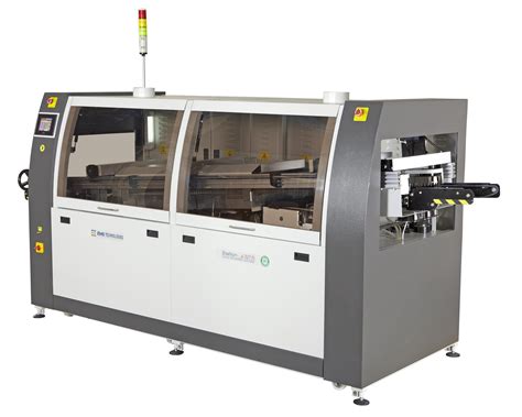
Wave Soldering Equipment
A typical wave soldering machine consists of several key components:
- Conveyor system: Transports the PCBs through the various stages of the wave soldering process.
- Fluxing station: Applies flux to the bottom side of the PCB to improve solder wetting and prevent oxidation.
- Preheating zone: Gradually heats the PCB to activate the flux and prevent thermal shock when the board contacts the molten solder.
- Solder pot: Contains the molten solder, which is typically an alloy of tin, lead, and sometimes silver.
- Solder nozzle: Shapes the molten solder into a standing wave as it flows over the weir.
- Cooling zone: Allows the soldered PCBs to cool down gradually to prevent thermal stress and ensure proper solder joint formation.

The Wave Soldering Process
The wave soldering process involves several steps, each contributing to the formation of reliable solder joints:
Step 1: PCB Preparation
Before wave soldering, the PCB must be properly prepared:
- Components are inserted into the through-holes on the top side of the board.
- The PCB is cleaned to remove any contaminants that may affect solder wetting.
- Solder masks and other protective coatings are applied to areas where soldering is not desired.
Step 2: Fluxing
The bottom side of the PCB is coated with flux, a chemical agent that improves solder wetting and prevents oxidation during the soldering process. Flux can be applied using various methods, such as spray fluxing, foam fluxing, or brush fluxing, depending on the specific requirements of the PCB Assembly.
Step 3: Preheating
The fluxed PCB enters the preheating zone, where it is gradually heated to a temperature typically between 100°C and 150°C. Preheating serves two main purposes:
- Activating the flux to remove oxides from the component leads and PCB pads.
- Reducing the thermal shock experienced by the components and PCB when they contact the molten solder wave.
Step 4: Wave Soldering
As the preheated PCB exits the preheating zone, it passes over the standing wave of molten solder. The solder wave is typically shaped by a specialized nozzle to ensure uniform contact with the PCB. The molten solder wets the component leads and PCB through-holes, forming a strong metallurgical bond.
The solder wave is usually composed of two distinct parts:
- Turbulent wave: The first part of the wave is turbulent, which helps to remove any remaining oxides and ensures good solder penetration into the through-holes.
- Laminar wave: The second part of the wave is laminar, which provides a smooth, controlled flow of solder over the PCB, minimizing the formation of solder bridges or icicles.
Step 5: Cooling
After passing over the solder wave, the PCB enters the cooling zone, where it is allowed to cool down gradually. Cooling helps to solidify the solder joints and prevent thermal stress on the components and PCB. Some wave soldering machines use air knives to remove excess solder from the PCB, reducing the need for post-soldering cleaning.
Step 6: Inspection and Cleaning
Once the PCB has cooled, it undergoes a visual inspection to check for any soldering defects, such as:
- Solder bridges: Unintended connections between adjacent pads or pins.
- Solder icicles: Sharp, pointy protrusions of excess solder.
- Insufficient solder: Incomplete or weak solder joints due to inadequate solder coverage.
If necessary, the soldered PCB may be cleaned to remove any residual flux or contaminants.

Factors Affecting Wave Soldering Quality
Several factors can influence the quality of wave soldered joints:
- Solder alloy composition: The choice of solder alloy affects the melting temperature, wetting behavior, and mechanical properties of the solder joints.
- Solder pot temperature: Maintaining the correct solder temperature is crucial for achieving proper solder wetting and preventing thermal damage to components.
- Conveyor speed: The speed at which the PCB passes over the solder wave determines the contact time between the molten solder and the PCB, affecting joint formation.
- Preheat temperature: Proper preheating is essential for activating the flux and preventing thermal shock during wave soldering.
- Flux selection: The type of flux used must be compatible with the PCB materials, components, and soldering process to ensure optimal solder wetting and joint reliability.
- PCB design: The layout and design of the PCB, including pad sizes, hole diameters, and component placement, can affect the quality of wave soldered joints.
Troubleshooting Common Wave Soldering Defects
Despite the automated nature of wave soldering, defects can still occur. Some common wave soldering defects and their potential causes include:
| Defect | Potential Causes |
|---|---|
| Solder bridges | – Excessive solder wave height – Insufficient board preheat – Inadequate flux coverage |
| Solder icicles | – Excessive solder wave height – Low conveyor speed – Incorrect solder nozzle angle |
| Insufficient solder | – Inadequate solder wave height – High conveyor speed – Poor flux activation |
| Solder balls | – Excessive flux residue – Contaminated solder pot – Incorrect preheat temperature |
To minimize wave soldering defects, it is essential to optimize the process parameters, maintain the equipment, and use high-quality materials.
Wave Soldering vs. Other Soldering Methods
While wave soldering is the most common method for soldering through-hole components, other soldering techniques are also used in the electronics manufacturing industry:
- Reflow soldering: Used primarily for surface mount components, reflow soldering involves applying solder paste to the PCB pads, placing the components, and heating the entire assembly to melt the solder and form the joints.
- Selective soldering: A targeted soldering method that uses a miniature solder wave or laser to solder specific components or areas on a PCB, often used for mixed-technology assemblies or rework.
- Hand soldering: A manual soldering process using a soldering iron, suitable for low-volume production, prototyping, or rework.
Each soldering method has its advantages and limitations, and the choice depends on factors such as component types, production volume, and assembly complexity.
Frequently Asked Questions (FAQ)
-
Q: What types of components can be soldered using wave soldering?
A: Wave soldering is primarily used for through-hole components, such as connectors, resistors, capacitors, and sockets. However, some surface mount components can also be wave soldered using specialized techniques, such as glue dots or adhesive tapes to hold the components in place during the process. -
Q: Can wave soldering be used for double-sided PCBs?
A: Yes, wave soldering can be used for double-sided PCBs, but it requires additional steps to prevent solder bridging on the top side of the board. This typically involves using a selective solder mask or solder thieves to control the solder flow and protect the top-side components. -
Q: What is the difference between leaded and lead-free wave soldering?
A: Leaded wave soldering uses solder alloys containing lead, typically Sn63Pb37 (63% tin, 37% lead), while lead-free wave soldering uses lead-free alloys, such as SAC305 (96.5% tin, 3% silver, 0.5% copper). Lead-free soldering requires higher process temperatures and may be more prone to certain defects, such as solder shrinkage voids. -
Q: How can I optimize my wave soldering process?
A: To optimize your wave soldering process, consider the following: - Fine-tune the process parameters, such as solder temperature, conveyor speed, and preheat temperature.
- Use high-quality materials, including PCBs, components, and solder alloys.
- Regularly maintain and calibrate your wave soldering equipment.
-
Monitor the process and perform quality control checks to identify and address any issues promptly.
-
Q: What safety precautions should be taken when operating a wave soldering machine?
A: Wave soldering involves high temperatures and molten metal, so safety precautions are essential: - Wear appropriate personal protective equipment (PPE), such as heat-resistant gloves, safety glasses, and protective clothing.
- Ensure proper ventilation to minimize exposure to fumes and vapors.
- Follow the manufacturer’s guidelines for operating and maintaining the wave soldering equipment.
- Train operators on safe work practices and emergency procedures.
Conclusion
Wave soldering is a highly efficient and reliable method for soldering through-hole components to PCBs in high-volume electronics manufacturing. By understanding the process, equipment, and factors affecting solder joint quality, manufacturers can optimize their wave soldering operations to produce consistent, high-quality assemblies. As technology advances and component packaging evolves, wave soldering continues to adapt and remain a critical process in the electronics industry.


Leave a Reply