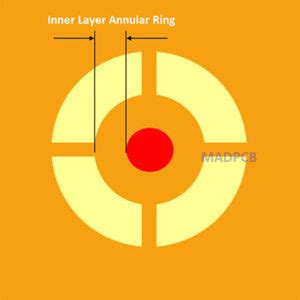
What are Annular Rings?
Annular rings, also known as fiducial rings or alignment rings, are concentric circular features on printed circuit boards (PCBs) that provide a reference point for automated assembly machines and optical inspection systems. These rings help ensure precise alignment and positioning of components during the manufacturing process, ultimately contributing to the overall quality and reliability of the PCB.
Key Characteristics of Annular Rings
Annular rings have several key characteristics that make them essential for PCB manufacturing:
-
Concentricity: The rings are concentric, meaning they share a common center point. This ensures consistent reference points for alignment.
-
Precision: Annular rings are designed with tight tolerances to provide accurate positioning and alignment of components.
-
Visibility: The rings are typically made using copper or other conductive materials, making them easily detectable by automated systems.
-
Standardization: The size and placement of annular rings are often standardized within the industry to ensure compatibility across different manufacturing processes and equipment.
The Role of Annular Rings in PCB Manufacturing
Alignment and Positioning
One of the primary functions of annular rings is to facilitate accurate alignment and positioning of components on the PCB. During the assembly process, automated pick-and-place machines use vision systems to locate the annular rings and determine the precise coordinates for placing components. This ensures that components are placed in the correct locations, with the proper orientation, and within the specified tolerances.
Quality Control and Inspection
Annular rings also play a crucial role in quality control and inspection processes. Automated optical inspection (AOI) systems use the rings as reference points to check for proper component placement, solder joint formation, and other quality factors. By comparing the actual position of components relative to the annular rings with the intended design, AOI systems can quickly identify any deviations or defects, allowing for early detection and correction of issues.
Design Considerations
When designing a PCB, it is essential to consider the placement and size of annular rings to ensure optimal manufacturability and reliability. Some key factors to consider include:
-
Ring Size: The size of the annular rings should be large enough to be easily detectable by automated systems, but not so large as to interfere with other components or routing.
-
Clearance: Sufficient clearance should be maintained around the annular rings to prevent short circuits or other issues during assembly.
-
Symmetry: Whenever possible, annular rings should be placed symmetrically on the PCB to balance the layout and improve overall manufacturability.
-
Quantity: The number of annular rings used should be sufficient to provide adequate reference points for alignment and inspection, without adding unnecessary complexity to the design.

Annular Ring Standards and Guidelines
Several industry standards and guidelines provide recommendations for the design and implementation of annular rings on PCBs. These standards help ensure consistency and compatibility across different manufacturing processes and equipment.
IPC Standards
The Association Connecting Electronics Industries (IPC) is a global trade association that develops standards for the electronic interconnect industry. Some key IPC standards related to annular rings include:
- IPC-7351: Provides guidelines for land pattern geometries, including annular ring dimensions and tolerances.
- IPC-A-600: Defines acceptability criteria for printed circuit boards, including annular ring requirements.
- IPC-SM-782: Covers surface mount design and land pattern standards, including recommendations for annular ring placement and sizing.
Manufacturer Guidelines
In addition to industry standards, individual PCB manufacturers may have their own guidelines and requirements for annular rings. These guidelines may take into account the specific capabilities and limitations of their manufacturing processes and equipment. It is essential to consult with the chosen manufacturer early in the design process to ensure compliance with their specific requirements.

Common Annular Ring Defects and Issues
While annular rings are designed to improve the quality and reliability of PCBs, several common defects and issues can arise during the manufacturing process. Understanding these issues can help designers and manufacturers take steps to prevent them and ensure the overall success of the project.
Misalignment
Misalignment occurs when the annular rings are not positioned correctly relative to the intended design. This can lead to components being placed in the wrong locations or with the wrong orientation, resulting in functional and reliability issues. Misalignment can be caused by factors such as incorrect CAD data, manufacturing process errors, or equipment malfunctions.
Breakout
Breakout refers to a condition where the copper plating on the annular ring is not fully formed or has separated from the base material. This can create an open circuit or high resistance connection, leading to electrical failures. Breakout can be caused by factors such as insufficient plating thickness, poor adhesion, or mechanical stress during assembly.
Shorts
Shorts occur when there is an unintended electrical connection between adjacent annular rings or other conductive features on the PCB. This can be caused by factors such as excessive solder, conductive contamination, or damage to the solder mask. Shorts can lead to electrical malfunctions, overheating, and other reliability issues.
Dimensional Variations
Dimensional variations refer to deviations in the size, shape, or position of the annular rings from the intended design. These variations can be caused by factors such as manufacturing process tolerances, material shrinkage, or changes in environmental conditions. Dimensional variations can impact the ability of automated systems to accurately locate and place components, leading to alignment and reliability issues.

Preventing and Mitigating Annular Ring Issues
To prevent and mitigate annular ring issues, designers and manufacturers can take several steps throughout the PCB development process.
Design for Manufacturability
During the design phase, it is essential to follow best practices for annular ring placement and sizing, as outlined in industry standards and manufacturer guidelines. This includes providing adequate clearance, maintaining symmetry, and using appropriate ring sizes and quantities. Designers should also communicate closely with the chosen manufacturer to ensure that the design is optimized for their specific processes and equipment.
Process Control
Manufacturers can implement robust process control measures to minimize the risk of annular ring defects and issues. This includes regular calibration and maintenance of equipment, monitoring of key process parameters, and implementation of statistical process control (SPC) techniques. By identifying and correcting process deviations early, manufacturers can prevent defects from occurring or propagating throughout the production run.
Quality Inspection
Thorough quality inspection is essential for detecting and mitigating annular ring issues. This includes visual inspection, automated optical inspection (AOI), and electrical testing. By catching defects early in the manufacturing process, corrective actions can be taken to prevent further issues and ensure the overall quality of the finished product.
Continuous Improvement
Finally, designers and manufacturers should strive for continuous improvement in their processes and practices related to annular rings. This includes staying up-to-date with the latest industry standards and guidelines, investing in new technologies and equipment, and collaborating with suppliers and partners to identify and implement best practices. By fostering a culture of continuous improvement, companies can drive ongoing enhancements in PCB Quality, reliability, and manufacturability.
Annular Ring FAQ
-
What is the purpose of annular rings on PCBs?
Annular rings serve as reference points for automated assembly machines and optical inspection systems, ensuring precise alignment and positioning of components during the manufacturing process. -
How do annular rings impact PCB quality and reliability?
Properly designed and implemented annular rings contribute to the overall quality and reliability of PCBs by enabling accurate component placement, facilitating automated inspection, and minimizing the risk of defects and issues. -
What factors should be considered when designing annular rings?
When designing annular rings, key factors to consider include ring size, clearance, symmetry, and quantity. It is also essential to follow industry standards and manufacturer guidelines to ensure optimal manufacturability and reliability. -
What are some common defects and issues associated with annular rings?
Common annular ring defects and issues include misalignment, breakout, shorts, and dimensional variations. These issues can lead to functional and reliability problems in the finished PCB. -
How can designers and manufacturers prevent and mitigate annular ring issues?
To prevent and mitigate annular ring issues, designers and manufacturers can focus on design for manufacturability, process control, quality inspection, and continuous improvement. By following best practices and collaborating closely throughout the PCB development process, companies can drive ongoing enhancements in quality, reliability, and manufacturability.
| Aspect | Recommendation |
|---|---|
| Ring Size | Large enough to be detectable, but not interfering with other components |
| Clearance | Sufficient clearance around rings to prevent short circuits |
| Symmetry | Place rings symmetrically on the PCB to balance the layout |
| Quantity | Use enough rings for adequate reference points, without unnecessary complexity |
By understanding the role of annular rings in PCB manufacturing, following best practices for their design and implementation, and proactively addressing common defects and issues, designers and manufacturers can ensure the success of their PCB projects. Through ongoing collaboration, innovation, and continuous improvement, the industry can continue to drive advancements in PCB quality, reliability, and manufacturability, ultimately enabling the development of more advanced and capable electronic products.


Leave a Reply