Introduction
Printed circuit boards (PCBs) are the backbone of modern electronics. They provide the foundation on which components are mounted and interconnected. Traditionally, PCBs have been made from rigid fiberglass. However, new materials and manufacturing techniques have enabled a new generation of ultra thin flexible PCBs that open up exciting possibilities for the future of electronics design.
In this article, we will explore what ultra thin flexible PCBs are, their benefits, how they are made, and emerging applications. We’ll also answer common questions about this promising new technology. Let’s dive in!
What Are Ultra Thin Flexible PCBs?

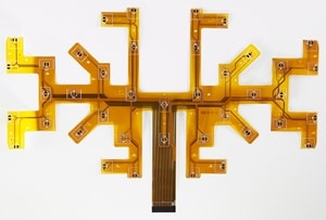
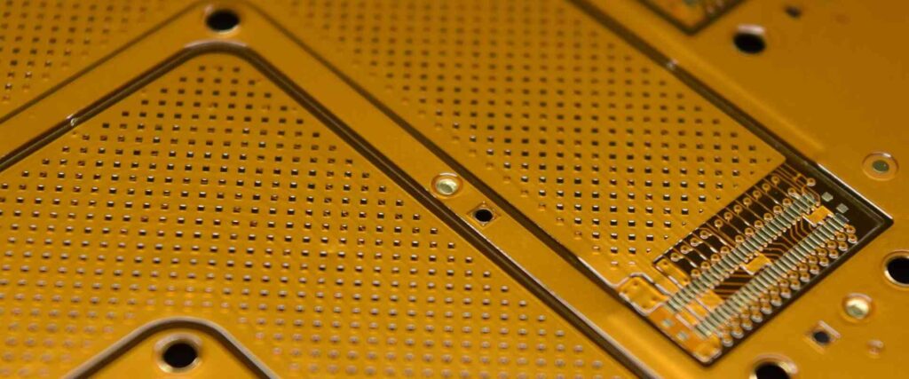
Ultra thin flexible PCBs, sometimes called flex circuits or flex PCBs, are circuit boards made from flexible polymer materials like polyimide instead of rigid fiberglass. This allows the boards to bend and flex while still providing electrical connections.
Flex PCBs can be made exceptionally thin – down to just 25 microns (0.001 inches) thick! That’s almost paper thin. By comparison, traditional rigid PCBs are typically 1.6 mm (0.063 inches) thick.
Benefits of Ultra Thin Flexible PCBs
The flexible nature and thin profile of flex PCBs provide some unique advantages:
- Lightweight: Flex PCBs weigh less than rigid boards
- Space savings: Flex PCBs take up less space and can fit into tight spaces
- Shape conforming: Flex PCBs can bend and shape to fit curvy surfaces
- Dynamic flexing: They can accommodate continuous motion and repeated bending
- Thin products: Allow creation of thinner electronic devices
- Reliability: Proven durability and interconnect reliability
In short, flex PCBs enable lighter, smaller, more dynamic, and more reliable electronics designs. Products can be made thinner, lighter, with greater functionality packed into a small space.
How Are Ultra Thin Flexible PCBs Made?
While the materials differ, ultra thin flex PCBs are manufactured using many of the same processes used for rigid PCB fabrication. Here is a high-level overview:
Step 1: Design
The PCB layout is designed using CAD (computer aided design) software. The designer must account for the flexibility of the material throughout the design process.
Step 2: Etching Copper
A layered sheet of flex material (like polyimide) is laminated with a thin layer of copper foil. Photolithographic processes are used to etch away unwanted copper, leaving behind the desired conductive traces.
Step 3: Die Cutting
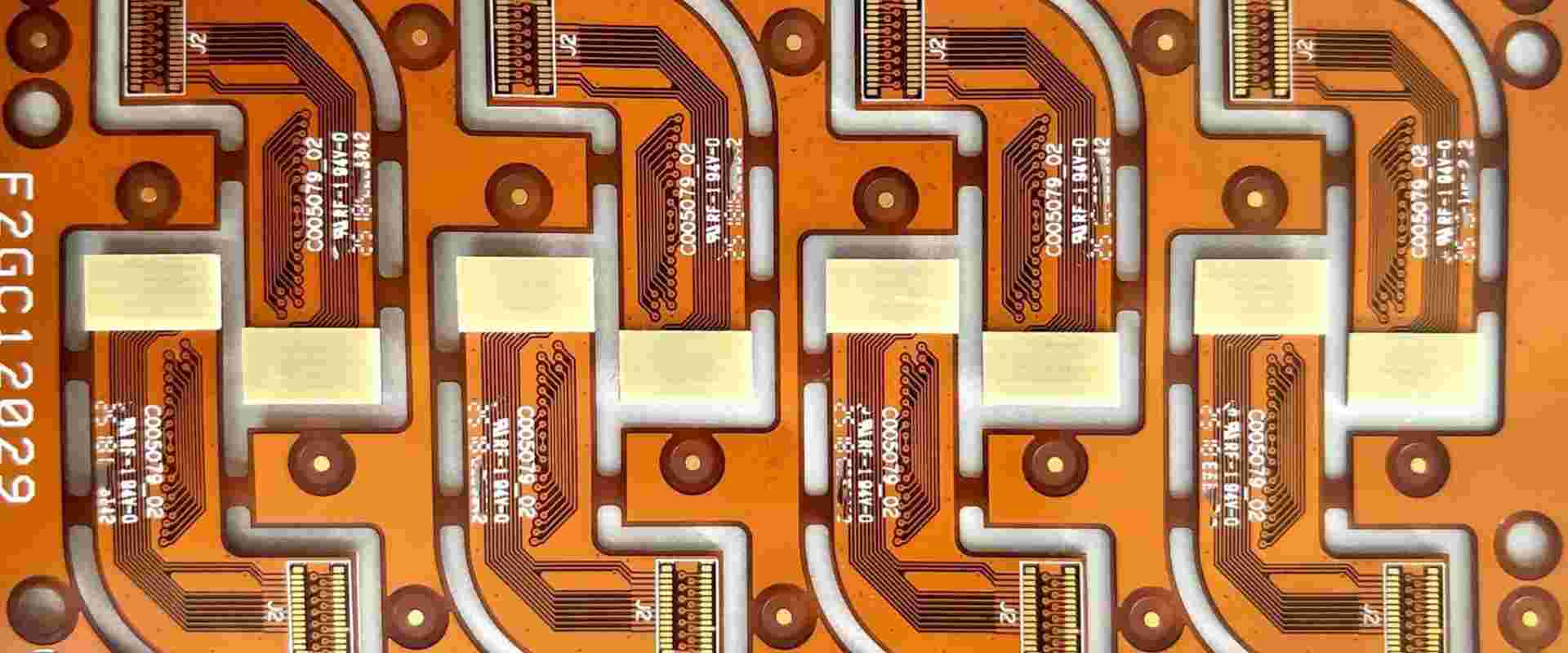
Once the conductive traces are defined, the PCB substrate is precision die cut into the required shapes.
Step 4: Component Assembly
Components are soldered onto the PCB using surface mount technology (SMT). The thin flexible material can be challenging to handle during assembly.
Step 5: Testing
Finished boards are visually inspected and electrically tested.
Step 6: Final Integration
The flex PCB is integrated into the end product, often connecting other rigid PCBs. Careful mechanical design is needed to prevent over-flexing.
Applications of Ultra Thin Flexible PCBs

The unique properties of flex PCBs make them well suited for many cutting edge applications:
Wearable Technology
Wearable devices need to be lightweight and conform to the body. Flex PCBs meet these requirements and are found in products like smart watches and fitness trackers.
Medical Devices
Medical devices like hearing aids and digital imaging systems need to fit into tight spaces. Thin flex PCBs can snake their way into confined areas.
Automotive
Cars are using more electronics but space is tight. Flex PCBs are ideal for connecting things like cameras, sensors, and displays inside vehicles while withstanding vibration.
Consumer Electronics
Phones, laptops, and other mobile consumer products continue to shrink. Flex PCBs allow for lighter and thinner product designs.
IoT and Wearables
As the Internet of Things and wearable tech grow, small flex PCBs will be needed to put intelligence into more everyday objects.
The applications are endless. Anytime size, weight, shape conforming, or movement is a factor, flex PCBs should be considered.
Ultra Thin Flexible PCBs FAQ
Here are answers to some frequently asked questions about this technology:
Are flex PCBs more expensive than rigid PCBs?
Generally yes, flex PCBs tend to cost more than rigid PCBs. The flexible material is more expensive than standard FR4 fiberglass. There is also more manual labor involved in assembly. However, the benefits often justify the costs in reduced product size/weight.
Are flex PCBs difficult to solder and assemble?
Yes, the flexible material can make assembly more challenging. Special fixtures are often needed to prevent warping during soldering. It takes practice to handle the thin flexible boards during assembly.
Can components be mounted on both sides of flex PCBs?
Yes, components can be assembled on both sides. This allows maximum use of space. Through-hole plating or conductive adhesives are used to connect both sides. Rigid sections may be screened onto the flex PCB for easier assembly.
How durable are ultra thin flex PCBs?
When designed properly, flex PCBs are extremely durable – tested to millions of flex cycles. The conductive traces are bonded to the flexible material and resistant to cracking. Proper mechanical design avoids over-flexing.
How small can flex PCB traces and spaces be?
Traces and spaces down to 10 microns are possible, allowing high density interconnections. Rigid sections allow even finer 5 micron traces.
Conclusion
Flex PCBs offer new possibilities for making electronics thinner, lighter, and more reliable. As products continue getting smaller, only limited by our imagination, ultra thin flex PCB technology will help make the next generation of incredible designs a reality. While costs are higher, the benefits often justify the investment. From wearable tech to car cameras to IoT sensors, flex PCBs are shaping the future of PCB design.


Leave a Reply