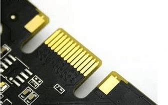
What are PCB+Gold+Fingers”>PCB Gold Fingers?
PCB gold fingers, also known as edge connectors or contact fingers, are the exposed metal contacts on the edge of a printed circuit board (PCB) that allow it to be plugged into a socket or connector. These gold-plated contacts provide a reliable and corrosion-resistant electrical connection between the PCB and the mating connector.
Gold fingers are commonly found on various types of PCBs, including:
- Computer memory modules (e.g., RAM, SSD)
- Expansion cards (e.g., graphics cards, sound cards)
- Motherboards
- Daughterboards
- Mezzanine cards
Advantages of Gold Fingers
Gold is the preferred material for PCB edge connectors due to its excellent properties:
- High conductivity
- Corrosion resistance
- Durability
- Low contact resistance
- Ease of soldering
These properties ensure a reliable and long-lasting electrical connection, even in harsh environments or with frequent insertions and removals.
PCB Gold Finger Plating Process
The process of applying gold plating to PCB fingers involves several steps to ensure a high-quality, durable finish.
1. PCB Design and Fabrication
Before the plating process can begin, the PCB must be designed and fabricated with the appropriate gold finger layout. The designer must consider factors such as:
- Finger pitch (distance between contacts)
- Finger width and length
- Clearance between fingers and surrounding components
- Soldermask and silkscreen markings
Once the design is finalized, the PCB is fabricated using standard processes, such as etching, drilling, and Solder Mask application.
2. Surface Preparation
To ensure proper adhesion of the gold plating, the PCB surface must be thoroughly cleaned and prepared. This typically involves the following steps:
- Degreasing: Removes oils, greases, and other contaminants from the surface using solvents or detergents.
- Micro-etching: Creates a slightly roughened surface to improve adhesion using a mild acid solution.
- Activation: Applies a thin layer of a catalytic material, such as palladium, to promote the deposition of the subsequent plating layers.
3. Nickel Plating
Before applying the gold plating, a layer of nickel is deposited onto the PCB fingers. Nickel serves as a barrier layer between the copper substrate and the gold plating, providing several benefits:
- Prevents the diffusion of copper into the gold layer, which can cause brittleness and reduced conductivity.
- Improves the wear resistance and durability of the gold plating.
- Enhances the overall corrosion resistance of the plated surface.
The nickel plating is typically applied using an electroplating process, where the PCB is immersed in a nickel electrolyte solution and an electric current is applied to deposit the nickel onto the surface.
4. Gold Plating
After the nickel plating, the gold layer is applied to the PCB fingers using a similar electroplating process. The PCB is immersed in a gold electrolyte solution, and an electric current is applied to deposit the gold onto the nickel surface.
The thickness of the gold plating is a critical factor in determining the performance and durability of the gold fingers. Typical gold plating thicknesses range from 0.05 to 2.0 micrometers (μm), depending on the application and requirements.
| Gold Plating Thickness | Typical Applications |
|---|---|
| 0.05 – 0.2 μm | Low-cost, short-life connectors |
| 0.2 – 0.5 μm | General-purpose connectors |
| 0.5 – 1.0 μm | High-reliability connectors |
| 1.0 – 2.0 μm | Extreme-durability connectors, military and aerospace applications |
5. Quality Control and Inspection
After the gold plating process is complete, the PCB undergoes thorough quality control and inspection to ensure that the gold fingers meet the required specifications. This may include:
- Visual inspection for surface defects, such as pits, nodules, or discoloration
- Thickness measurement using X-ray fluorescence (XRF) or other methods
- Adhesion testing using tape or scratch tests
- Solderability Testing
- Electrical resistance measurement
PCBs that pass the quality control checks are then packaged and shipped to the customer for assembly and use.

Frequently Asked Questions (FAQ)
1. What is the difference between hard and soft gold plating?
Hard gold plating contains a small amount of cobalt or nickel to increase its hardness and wear resistance. It is typically used for high-wear applications, such as connectors that undergo frequent insertions and removals. Soft gold plating, on the other hand, is pure gold and is more ductile and malleable. It is often used for wire bonding or other applications where the gold surface must be deformed.
2. Can gold fingers be repaired if damaged?
In some cases, damaged gold fingers can be repaired by carefully sanding or filing the surface to remove the damaged area and then applying a new layer of gold plating. However, this process is delicate and may not always be feasible, especially for severe damage or high-precision applications.
3. Are there any alternatives to gold plating for PCB fingers?
While gold is the most common and preferred material for PCB fingers, some alternatives include:
- Palladium-nickel alloy plating
- Silver plating
- Tin plating
These alternatives may be used in lower-cost or less-demanding applications, but they may not provide the same level of performance and durability as gold plating.
4. How does the gold finger pitch affect PCB design?
The pitch of the gold fingers determines the maximum number of contacts that can fit along the edge of the PCB. A smaller pitch allows for more contacts in a given space but requires more precise manufacturing and assembly processes. The pitch also affects the connector design and the overall system layout, as the mating connector must have matching dimensions and spacing.
5. What environmental factors can affect the durability of gold fingers?
Several environmental factors can impact the durability and performance of gold fingers, including:
- Temperature: Extreme temperatures or thermal cycling can cause stress and wear on the plated surfaces.
- Humidity: High humidity can promote corrosion, especially if the gold plating is thin or porous.
- Chemical exposure: Exposure to harsh chemicals, such as acids or solvents, can degrade the gold plating and cause failures.
- Mechanical stress: Frequent insertions and removals, vibration, or other mechanical stresses can cause wear and damage to the gold fingers over time.
Proper design, material selection, and protective measures can help mitigate these environmental factors and ensure the long-term reliability of PCB gold fingers.

Conclusion
PCB gold fingers play a crucial role in providing reliable, high-performance electrical connections between PCBs and mating connectors. The gold plating process, which involves surface preparation, nickel plating, and gold deposition, ensures a durable and corrosion-resistant surface finish that can withstand the demands of various applications.
By understanding the properties, advantages, and manufacturing processes behind PCB gold fingers, designers and engineers can make informed decisions when specifying and using these critical components in their electronic systems.


Leave a Reply