What is Solder Mask?
Solder mask, also known as solder resist or solder stop mask, is a thin layer of polymer that is applied to the copper traces of a printed circuit board (PCB). Its primary purpose is to prevent solder from bridging between conductors during the soldering process, which could lead to short circuits and other issues. Solder mask also provides protection against oxidation and corrosion, improving the overall durability of the PCB.
Composition of Solder Mask
Solder mask is typically composed of a photoimageable material, such as:
- Epoxy
- Acrylic
- Polyimide
- Urethane
These materials are mixed with fillers, pigments, and other additives to achieve the desired properties, such as color, gloss, and flame retardancy.
Application Process
The application of solder mask involves several steps:
-
Cleaning: The PCB is thoroughly cleaned to remove any contaminants that could affect the adhesion of the solder mask.
-
Application: The solder mask is applied to the PCB using one of the following methods:
- Screen printing
- Spraying
- Curtain coating
-
Electrostatic deposition
-
Curing: The solder mask is cured using heat, ultraviolet light, or a combination of both, depending on the type of material used.
-
Developing: The unexposed areas of the solder mask are removed using a developer solution, leaving behind the desired pattern.
-
Final Curing: The PCB undergoes a final curing process to ensure the solder mask is fully hardened and adhered to the surface.
Types of Solder Mask
There are several types of solder mask available, each with its own unique properties and applications:
Liquid Photoimageable Solder Mask (LPSM)
LPSM is the most common type of solder mask used in the PCB industry. It is applied as a liquid and then exposed to ultraviolet light through a photomask, which hardens the exposed areas. The unexposed areas are then removed using a developer solution.
Advantages of LPSM:
– High resolution
– Excellent adhesion
– Good chemical resistance
– Available in a variety of colors
Disadvantages of LPSM:
– Requires specialized equipment for application and curing
– Can be more expensive than other types of solder mask
Dry Film Solder Mask (DFSM)
DFSM is a solid film that is laminated onto the PCB using heat and pressure. It is then exposed to ultraviolet light through a photomask, which hardens the exposed areas. The unexposed areas are removed using a developer solution.
Advantages of DFSM:
– Easier to apply than LPSM
– More cost-effective for high-volume production
– Good chemical resistance
Disadvantages of DFSM:
– Lower resolution compared to LPSM
– Limited color options
Peelable Solder Mask (PSM)
PSM is a temporary solder mask that can be easily removed after the soldering process. It is typically used for prototype or low-volume production runs.
Advantages of PSM:
– Easy to apply and remove
– Cost-effective for small batches
– Allows for easy rework and modification
Disadvantages of PSM:
– Not suitable for high-volume production
– Limited durability and chemical resistance

Solder Mask Colors
Solder mask is available in a variety of colors, with green being the most common. Other popular colors include:
- Blue
- Red
- Yellow
- Black
- White
The choice of color is often dictated by the specific application or industry standards. For example, in the automotive industry, blue solder mask is commonly used for high-voltage applications, while red is used for low-voltage applications.
| Color | Application |
|---|---|
| Green | General-purpose, most common color |
| Blue | Automotive (high-voltage), aerospace, military |
| Red | Automotive (low-voltage), consumer electronics |
| Yellow | High-reliability applications, aerospace, military |
| Black | High-end consumer electronics, aesthetics |
| White | LED lighting, reflective surfaces, aesthetics |

Solder Mask Properties
When selecting a solder mask for a specific application, several properties should be considered:
Electrical Properties
-
Dielectric Strength: The ability of the solder mask to withstand high voltages without breaking down. Higher dielectric strength is required for high-voltage applications.
-
Insulation Resistance: The resistance of the solder mask to the flow of electrical current. Higher insulation resistance is desirable to prevent leakage currents.
Mechanical Properties
-
Adhesion: The ability of the solder mask to adhere to the PCB surface. Good adhesion is essential for long-term reliability.
-
Hardness: The resistance of the solder mask to indentation or scratching. Higher hardness is desirable for improved durability.
-
Flexibility: The ability of the solder mask to withstand bending and flexing without cracking or delaminating. Flexibility is important for applications where the PCB may be subjected to mechanical stress.
Chemical Properties
-
Resistance to Solvents: The ability of the solder mask to withstand exposure to various solvents, such as isopropyl alcohol and acetone, without degrading.
-
Resistance to Acids and Bases: The ability of the solder mask to withstand exposure to acidic and basic solutions without degrading.
-
Flammability: The resistance of the solder mask to ignition and flame spread. Some applications may require solder mask with improved flame retardancy.
Thermal Properties
-
Glass Transition Temperature (Tg): The temperature at which the solder mask transitions from a rigid, glassy state to a soft, rubbery state. A higher Tg is desirable for applications with elevated operating temperatures.
-
Coefficient of Thermal Expansion (CTE): The rate at which the solder mask expands with increasing temperature. A lower CTE is desirable to minimize stress on the PCB during temperature cycling.
-
Thermal Conductivity: The ability of the solder mask to conduct heat. Higher thermal conductivity can help dissipate heat from the PCB, improving overall thermal performance.

Solder Mask Design Considerations
When designing a PCB with solder mask, several factors should be considered to ensure optimal performance and manufacturability:
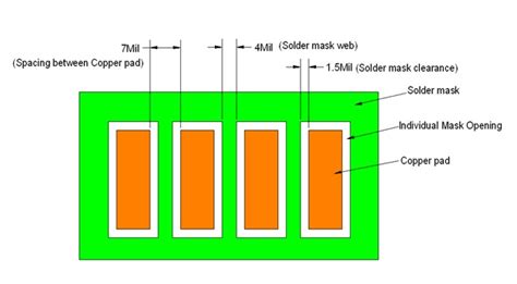
Solder Mask Clearance
Solder mask clearance refers to the minimum distance between the edge of a pad or trace and the edge of the solder mask opening. Adequate clearance is necessary to ensure proper solder wetting and to prevent solder bridging.
| Pad Size (mm) | Minimum Solder Mask Clearance (mm) |
|---|---|
| < 0.5 | 0.05 |
| 0.5 – 1.0 | 0.075 |
| 1.0 – 2.0 | 0.1 |
| > 2.0 | 0.15 |
Solder Mask Sliver
Solder mask sliver refers to the minimum width of solder mask between two adjacent openings. If the sliver is too narrow, it may break off during the solder mask application process, leading to short circuits.
| Solder Mask Type | Minimum Solder Mask Sliver Width (mm) |
|---|---|
| LPSM | 0.1 |
| DFSM | 0.15 |
Solder Mask Thickness
The thickness of the solder mask can affect its electrical and mechanical properties. Thicker solder mask provides better insulation and durability but may be more difficult to apply evenly.
| Solder Mask Type | Typical Thickness Range (µm) |
|---|---|
| LPSM | 12 – 50 |
| DFSM | 25 – 50 |
Solder Mask Color and Finish
The choice of solder mask color and finish can impact the appearance and functionality of the PCB. Consider the following:
-
Gloss Level: A high-gloss finish can improve the aesthetic appeal of the PCB but may make it more difficult to inspect and rework. A matte finish is often preferred for easier handling and inspection.
-
Color Consistency: Ensure that the solder mask color is consistent across the entire PCB and from batch to batch. Inconsistent color can indicate issues with the solder mask application process.
-
Transparency: Some applications may require transparent or semi-transparent solder mask to allow for inspection of the underlying circuitry. In such cases, a clear or translucent solder mask may be used.
Frequently Asked Questions (FAQ)
1. What is the purpose of solder mask on a PCB?
The primary purpose of solder mask is to prevent solder from bridging between conductors during the soldering process, which could lead to short circuits and other issues. Solder mask also provides protection against oxidation and corrosion, improving the overall durability of the PCB.
2. What is the most common color for solder mask?
Green is the most common color for solder mask, followed by blue, red, yellow, black, and white. The choice of color is often dictated by the specific application or industry standards.
3. What is the difference between liquid photoimageable solder mask (LPSM) and dry film solder mask (DFSM)?
LPSM is applied as a liquid and then exposed to ultraviolet light through a photomask, which hardens the exposed areas. DFSM is a solid film that is laminated onto the PCB using heat and pressure, then exposed to ultraviolet light through a photomask. LPSM offers higher resolution and better adhesion, while DFSM is easier to apply and more cost-effective for high-volume production.
4. How does solder mask affect the electrical properties of a PCB?
Solder mask serves as an insulating layer on the PCB, increasing the dielectric strength and insulation resistance. This helps prevent leakage currents and improves the overall electrical performance of the PCB.
5. What factors should be considered when designing a PCB with solder mask?
When designing a PCB with solder mask, consider factors such as solder mask clearance (the minimum distance between the edge of a pad or trace and the edge of the solder mask opening), solder mask sliver (the minimum width of solder mask between two adjacent openings), solder mask thickness, and the choice of color and finish. Proper design considerations help ensure optimal performance and manufacturability of the PCB.


Leave a Reply