Introduction to the UC3844 PWM Controller
The UC3844 is a fixed-frequency pulse width modulation (PWM) controller integrated circuit commonly used in switch mode power supplies (SMPS). It provides an easy and cost-effective solution for controlling and regulating the output voltage in offline power converters and adapters.
Key features of the UC3844 include:
– Wide operating supply voltage range (8V to 36V)
– Built-in oscillator with 500ns max delay
– Voltage feed-forward compensation
– Precision 5V reference voltage
– Under-voltage lockout and soft-start
– Latching PWM to prevent multiple pulses
– Totem-pole output
The UC3844 is suitable for flyback, forward, and push-pull converter topologies with output powers up to 200W. Its electrical characteristics are guaranteed over the extended industrial temperature range of -40°C to +85°C.
Block Diagram and Pinout
Here is the functional block diagram for the UC3844:
[UC3844 block diagram image]
And the pinout:
| Pin No. | Pin Name | Description |
|---|---|---|
| 1 | COMP | Error amplifier output and PWM comparator input |
| 2 | FB | Feedback voltage input |
| 3 | ISENSE | Current sense input |
| 4 | RT/CT | Oscillator timing resistor and capacitor input |
| 5 | GND | Ground |
| 6 | OUT | Output to MOSFET gate driver |
| 7 | VCC | Positive supply voltage |
| 8 | REF | 5V reference output |
How the UC3844 Works
Power Supply Control Loop
The UC3844 implements a voltage-mode control loop to regulate the converter output voltage. Key components that make up the control loop include:
- Error amplifier
- Voltage reference
- PWM comparator
- Oscillator
- Output driver
The feedback voltage from the converter output is compared to an internal precision reference voltage by the error amplifier. The output of the error amplifier (COMP pin) is then fed into the PWM comparator.
The oscillator generates a fixed-frequency sawtooth waveform that sets the PWM switching frequency, typically between 20kHz-500kHz. This sawtooth is also fed into the PWM comparator.
The PWM comparator output goes high when the sawtooth rises above the error amplifier output voltage. This signal then passes through the output driver to switch the external MOSFET on and off at a duty cycle that maintains the converter output voltage at the desired regulated value.
Voltage Feed-Forward
The UC3844 implements voltage feed-forward by using the oscillator timing capacitor charge current to provide a sample of the converter’s input voltage. This allows the PWM duty cycle to proactively compensate for input line voltage changes, improving line regulation and transient response.
Current Limiting
The ISENSE pin is used to monitor the converter primary current for implementing cycle-by-cycle current limiting. If the ISENSE pin voltage exceeds 1V, the output driver is turned off until the next clock cycle.
Soft-Start
The UC3844 provides soft-start to control the output voltage rise time at turn-on and limit inrush currents. An external capacitor from COMP to GND sets the soft-start time constant. On power-up, COMP is discharged to GND and slowly charges to its steady-state value.

Design Considerations
Setting the Switching Frequency
The switching frequency is programmed by the timing resistor (RT) and capacitor (CT) connected to the RT/CT pin. The switching period is approximately:
T ≈ 1.72 RC
where R is in ohms and C is in farads. Typical frequencies range from 20kHz to 500kHz.
Higher frequencies allow smaller inductors and capacitors to be used, but increase MOSFET switching losses. Frequencies above 200kHz may require additional slope compensation for stability.
Selecting the Inductors
Inductor selection is a key part of converter design. The inductor value must provide sufficient energy storage while keeping peak currents below the saturation and maximum ratings.
For a discontinuous Flyback Converter, the minimum primary inductance to maintain discontinuous current mode is:
Lmin = [(Vin_max × D_max) / (Ipri_peak × fsw)] × (Vout + Vf) / (Vin_min – Vsw)
where:
– Vin_max = Maximum input voltage
– D_max = Maximum duty cycle
– Ipri_peak = Maximum primary peak current
– fsw = Switching frequency
– Vout = Output voltage
– Vf = Output diode forward voltage
– Vsw = MOSFET on-state voltage
The number of inductor turns is then selected based on the desired maximum flux density.
For continuous mode flyback and forward converters, there are different equations for sizing the inductance and number of turns.
Transformer Design
For isolated topologies like flyback converters, a coupled inductor or transformer is used to provide isolation and step up/down the voltage. Key transformer specs include:
- Inductance
- Turns ratio
- Leakage inductance
- Inter-winding capacitance
- Wire current density
- Temperature rise
The primary inductance is sized to provide sufficient energy storage. The turns ratio is selected to achieve the desired output voltage:
Ns/Np = (Vout + Vf) / (Vin × D_max)
where Ns and Np are the secondary and primary number of turns.
Leakage inductance and inter-winding capacitance must be minimized to reduce ringing and shorten voltage spikes.
Feedback Loop Compensation
The feedback loop must be compensated for good transient response and output voltage regulation.
Type 2 compensation using two poles and one zero is commonly used. The compensation components (resistors and capacitors) are selected based on the converter transfer function to achieve at least 45° of phase margin.
Equations for selecting type 2 compensation component values can be found in most power supply control design books and application notes.

Application Circuits
Here are some typical application circuits using the UC3844:
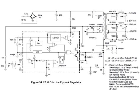
Flyback Converter
[Flyback schematic image]
This discontinuous conduction mode (DCM) flyback converter provides galvanic isolation and voltage step-up/down. It is suitable for low-mid power levels (5-150W).
Forward Converter
[Forward schematic image]
The forward converter is another popular isolated topology that uses the transformer for energy transfer rather than energy storage like the flyback. It is more suitable for higher power levels (50-500W).
Synchronous Buck Converter
[Buck synchronous schematic image]
Non-isolated buck converters are a simple way to step-down voltages at high efficiency. Using a synchronous rectifier (MOSFET) rather than a diode improves efficiency at low voltages.

UC3844 vs UC3845
The UC3844 has an NPN totem-pole output for driving N-channel MOSFETs. Its companion part, the UC3845, has a PNP totem-pole for driving P-channel MOSFETs.
Functionally, they are the same, and the choice between the two depends on whether an N-channel or P-channel switching MOSFET makes the most sense for the power supply design.
Frequently Asked Questions (FAQ)
What are the differences between the UC3842 and UC3844?
The UC3842 is an earlier-generation part that is similar to the UC3844. Key differences are:
- UC3842 has a wider oscillator frequency range (100Hz to 500kHz)
- UC3842 has max duty cycle limiting
- UC3844 adds voltage feed-forward compensation
- UC3844 has a higher operating supply current
In general, the UC3844 is a newer, improved part, but the UC3842 is still used in some designs.
Can the UC3844 be used for resonant converters?
The UC3844 is designed for hard-switched PWM converters and is not suitable for resonant topologies. The UC3861 and UC3863 controllers have features tailored for resonant mode converters.
How do you select the current sense resistor?
The current sense resistor (Rs) sets the maximum peak primary current. It is calculated as:
Rs = 1V / Ipri_peak
where 1V is the UC3844 current limit threshold voltage. The resistor power dissipation is:
Prs = (Ipri_peak^2 × Rs) × D_max
So the resistor must be sized to handle this power. Typical values are in the 0.1-0.5 ohm range.
What causes the UC3844 to go into UVLO?
The UC3844 has an under-voltage lockout (UVLO) circuit that shuts down the controller if the VCC supply voltage falls below a minimum threshold, typically around 8.5V.
Potential causes of UVLO include:
– Insufficient startup current from the high-voltage bias supply
– Overload or short circuit on the VCC pin
– Excessive output cable length or capacitance loading VCC
How do you design the hold-up time capacitor?
For offline AC-DC converters, a bulk capacitor is used after the input bridge rectifier to provide hold-up time – the amount of time the output voltage remains in regulation after the AC input is lost.
The required hold-up capacitance is:
Cout = 2 × P × Thold / (Vin_min^2 – Vin_uv^2)
where:
– P = output power
– Thold = desired hold-up time
– Vin_min = minimum operating input voltage
– Vin_uv = bulk voltage where undervoltage fault occurs
The capacitor must be rated for the full input voltage plus margin. Typical values are in the 100-1000uF range. Aluminum electrolytics or high-value MPPF film caps are commonly used.
Conclusion
The UC3844 is a versatile and easy-to-use PWM controller IC for low-medium power SMPS applications. Its voltage-mode control, voltage feed-forward, current limiting, and protection features simplify the design of efficient and robust isolated and non-isolated converters.
By understanding how to select the switching frequency, inductance, and compensation values, designers can quickly develop power converters based on the UC3844 to meet their application needs.


Leave a Reply