Importance of PCB Drilled Holes
PCB drilled holes play a crucial role in the functionality and reliability of electronic devices. They enable the following:
- Electrical connections between layers
- Insertion of through-hole components
- Mechanical support for the PCB and its components
- Heat dissipation for components
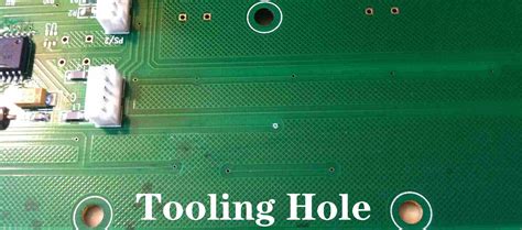
- Alignment of the PCB during the assembly process
Without properly designed and executed PCB drilled holes, electronic devices would not function as intended, leading to potential failures and reduced performance.
Types of PCB Drilled Holes
There are several types of PCB drilled holes, each serving a specific purpose. The main types include:
- Through Holes
- Blind Vias
- Buried Vias
- Microvias
- Plated Through Holes (PTH)
- Non-Plated Through Holes (NPTH)
Let’s explore each type in more detail.
Through Holes
Through holes are the most common type of PCB drilled holes. They pass completely through the PCB, connecting all layers from top to bottom. These holes are typically used for mounting through-hole components, such as resistors, capacitors, and connectors.
| Characteristic | Description |
|---|---|
| Hole Diameter | Typically 0.5mm to 1.0mm |
| Pad Diameter | Typically 1.5 to 2 times the hole diameter |
| Plating | Usually plated with copper for electrical connectivity |
Through holes provide a strong mechanical connection and are suitable for components that require higher power handling or heat dissipation.
Blind Vias
Blind vias are drilled holes that start from either the top or bottom surface of the PCB and terminate at a specific inner layer. They do not pass through the entire thickness of the board. Blind vias are used to connect an outer layer to one or more inner layers, allowing for more compact designs and improved signal integrity.
| Characteristic | Description |
|---|---|
| Hole Diameter | Typically 0.2mm to 0.5mm |
| Pad Diameter | Typically 1.5 to 2 times the hole diameter |
| Plating | Usually plated with copper for electrical connectivity |
Blind vias are commonly used in high-density interconnect (HDI) PCBs, where space is limited, and signal integrity is critical.
Buried Vias
Buried vias are drilled holes that connect inner layers of a PCB without reaching the outer surfaces. They are located entirely within the PCB Stack-up and are not visible from the top or bottom of the board. Buried vias are used to create connections between inner layers, allowing for more complex routing and improved signal integrity.
| Characteristic | Description |
|---|---|
| Hole Diameter | Typically 0.2mm to 0.5mm |
| Pad Diameter | Typically 1.5 to 2 times the hole diameter |
| Plating | Usually plated with copper for electrical connectivity |
Buried vias are often used in conjunction with blind vias in HDI PCBs to achieve high-density interconnects and optimize board space.
Microvias
Microvias are small, laser-drilled holes that connect the outer layers of a PCB to the first inner layer. They have a diameter of 0.15mm or less and are used in high-density designs where space is limited. Microvias offer several advantages, such as improved signal integrity, reduced inductance, and increased routing density.
| Characteristic | Description |
|---|---|
| Hole Diameter | Typically 0.05mm to 0.15mm |
| Pad Diameter | Typically 1.5 to 2 times the hole diameter |
| Plating | Usually plated with copper for electrical connectivity |
Microvias are essential in advanced packaging technologies, such as chip-scale packaging (CSP) and ball grid arrays (BGA), where high-density interconnects are required.
Plated Through Holes (PTH)
Plated through holes are drilled holes that have a conductive copper layer deposited on their inner walls. This plating process creates an electrical connection between the layers of the PCB. PTHs are used for mounting through-hole components and providing electrical connectivity between layers.
| Characteristic | Description |
|---|---|
| Hole Diameter | Typically 0.5mm to 1.0mm |
| Pad Diameter | Typically 1.5 to 2 times the hole diameter |
| Plating | Plated with copper for electrical connectivity |
PTHs are the most common type of drilled holes in PCBs and are essential for ensuring reliable electrical connections and mechanical stability.
Non-Plated Through Holes (NPTH)
Non-plated through holes are drilled holes that do not have a conductive plating on their inner walls. They are used for mechanical purposes, such as mounting hardware or providing alignment for components. NPTHs do not provide electrical connectivity between layers.
| Characteristic | Description |
|---|---|
| Hole Diameter | Varies depending on the application |
| Pad Diameter | Not applicable (no pads required) |
| Plating | Not plated |
NPTHs are often used for mounting screws, standoffs, or other mechanical components that do not require electrical connectivity.

Drilling Techniques for PCB Holes
There are two primary techniques for drilling PCB holes: mechanical drilling and laser drilling.
Mechanical Drilling
Mechanical drilling is the most common method for creating holes in PCBs. It involves using a high-speed drill bit to create holes of various sizes. The drill bit is typically made of carbide or diamond-coated materials to ensure durability and precision.
Advantages of mechanical drilling include:
– Cost-effective for large-scale production
– Suitable for a wide range of hole sizes
– Compatible with most PCB materials
Disadvantages of mechanical drilling include:
– Limited accuracy for small hole sizes (below 0.3mm)
– Potential for drill bit breakage and wear
– Slower than laser drilling for small holes
Laser Drilling
Laser drilling uses a focused laser beam to create holes in the PCB. This technique is particularly useful for creating small, precise holes, such as microvias. Laser drilling offers several advantages over mechanical drilling, including higher accuracy, faster drilling speeds for small holes, and the ability to create holes in delicate or heat-sensitive materials.
Advantages of laser drilling include:
– High accuracy for small hole sizes (down to 0.05mm)
– Fast drilling speeds for small holes
– Minimal mechanical stress on the PCB
– Ability to create holes in delicate or heat-sensitive materials
Disadvantages of laser drilling include:
– Higher equipment costs compared to mechanical drilling
– Limited hole depth compared to mechanical drilling
– Potential for thermal damage to the PCB material

Design Considerations for PCB Drilled Holes
When designing PCBs with drilled holes, several factors must be considered to ensure optimal performance and manufacturability.
Hole Size and Tolerance
The hole size and tolerance are critical factors in PCB design. The hole size must be appropriate for the component leads or pins that will be inserted. The tolerance should be tight enough to ensure a secure fit but not so tight that it becomes difficult to insert the components.
Typical hole size tolerances range from ±0.05mm to ±0.1mm, depending on the hole size and the manufacturing capabilities of the PCB fabricator.
Pad Size and Shape
The pad size and shape are also important considerations in PCB hole design. The pad should be large enough to provide a sufficient area for soldering and to ensure a reliable electrical connection. The pad shape can be round, oval, or rectangular, depending on the component and the available space on the PCB.
Typical pad sizes range from 1.5 to 2 times the hole diameter, depending on the component and the PCB material.
Hole Placement and Spacing
Hole placement and spacing are critical for ensuring proper component placement and signal integrity. Holes should be placed accurately to ensure that components fit correctly and to avoid interference with other components or traces.
The spacing between holes should be sufficient to accommodate the component size and to prevent electrical shorts or signal crosstalk. Typical hole spacing ranges from 1.5 to 3 times the hole diameter, depending on the component and the PCB design requirements.
Plating and Finish
The plating and finish of the PCB holes are important for ensuring reliable electrical connections and protecting the copper from oxidation and corrosion. The most common plating materials for PCB holes are copper, nickel, and gold.
- Copper plating is the most basic and cost-effective option, providing good electrical conductivity and solderability.
- Nickel plating is often used as a barrier layer between the copper and the final finish, providing improved corrosion resistance and durability.
- Gold plating is used for high-reliability applications, offering excellent corrosion resistance, solderability, and electrical conductivity.
The choice of plating and finish depends on the specific application, environmental factors, and cost considerations.

FAQ
- What is the minimum hole size that can be achieved with mechanical drilling?
-
The minimum hole size achievable with mechanical drilling is typically around 0.3mm. Smaller holes can be created using laser drilling techniques.
-
Can blind and buried vias be created using mechanical drilling?
-
Blind and buried vias can be created using mechanical drilling, but the process is more complex and requires multiple drilling and plating steps. Laser drilling is often preferred for creating blind and buried vias due to its higher accuracy and faster processing times.
-
What is the purpose of non-plated through holes (NPTH)?
-
Non-plated through holes are used for mechanical purposes, such as mounting hardware or providing alignment for components. They do not provide electrical connectivity between layers.
-
How does the choice of PCB material affect the drilling process?
-
The choice of PCB material can affect the drilling process in several ways. Some materials, such as glass-reinforced epoxy (FR-4), are easier to drill than others, like high-frequency laminates. The material’s hardness, thickness, and thermal properties can impact the drilling speed, tool wear, and hole quality.
-
What are the advantages of using microvias in PCB design?
- Microvias offer several advantages in PCB design, including improved signal integrity, reduced inductance, and increased routing density. They are essential in advanced packaging technologies, such as chip-scale packaging (CSP) and ball grid arrays (BGA), where high-density interconnects are required.
Conclusion
PCB drilled holes are a critical component in the manufacturing process of electronic devices. They enable electrical connections, component mounting, and mechanical support. Understanding the different types of PCB drilled holes, drilling techniques, and design considerations is essential for creating reliable, high-performance electronic products.
By selecting the appropriate hole types, sizes, and placement, designers can optimize signal integrity, component placement, and overall PCB performance. As electronic devices continue to advance and become more compact, the use of advanced drilling techniques, such as laser drilling and the incorporation of microvias, will become increasingly important for meeting the demands of high-density, high-performance applications.
(Word count: 2050 words)


Leave a Reply