Introduction to PCB-Types
Printed Circuit Boards (PCBs) are the backbone of modern electronics. These boards are used to mechanically support and electrically connect electronic components using conductive tracks, pads, and other features etched from copper sheets laminated onto a non-conductive substrate. PCBs have revolutionized the electronics industry by providing a reliable and efficient way to manufacture complex electronic circuits.
There are several types of PCBs, each with its own unique characteristics and applications. In this article, we will explore the various types of PCBs, their manufacturing processes, and their use cases.
Single-Sided PCB
What is a Single-Sided PCB?
A single-sided PCB, also known as a Single-Layer PCB, is a type of printed circuit board that has conductive tracks and components on only one side of the board. The other side of the board is typically left bare or covered with a solder mask to protect the copper traces from oxidation and short-circuiting.
Manufacturing Process
The manufacturing process for single-sided PCBs involves the following steps:
- Designing the PCB layout using a CAD software
- Printing the design onto a photoresist film
- Laminating the photoresist film onto a copper-clad board
- Exposing the board to UV light to harden the photoresist
- Developing the board to remove the unhardened photoresist
- Etching the board to remove the unwanted copper
- Drilling holes for through-hole components
- Applying a solder mask and silkscreen
- Testing and inspecting the board
Applications
Single-sided PCBs are commonly used in simple electronic devices such as:
- Calculators
- Radios
- Timing circuits
- LED displays
- Power supplies
Advantages and Disadvantages
Advantages:
– Low cost
– Easy to design and manufacture
– Suitable for low-complexity circuits
Disadvantages:
– Limited routing options
– Low component density
– Not suitable for high-frequency applications

Double-Sided PCB
What is a Double-Sided PCB?
A double-sided PCB, also known as a two-layer PCB, is a type of printed circuit board that has conductive tracks and components on both sides of the board. The two layers are connected using through-hole vias, which allow signals to pass from one side of the board to the other.
Manufacturing Process
The manufacturing process for double-sided PCBs is similar to that of single-sided PCBs, with a few additional steps:
- Designing the PCB layout using a CAD software
- Printing the design onto two photoresist films (one for each side)
- Laminating the photoresist films onto both sides of a copper-clad board
- Exposing the board to UV light to harden the photoresist
- Developing the board to remove the unhardened photoresist
- Etching the board to remove the unwanted copper
- Drilling holes for through-hole components and vias
- Plating the holes to create electrical connections between the layers
- Applying a solder mask and silkscreen
- Testing and inspecting the board
Applications
Double-sided PCBs are commonly used in moderately complex electronic devices such as:
- Amplifiers
- Power supplies
- Automotive electronics
- Industrial controls
- Medical devices
Advantages and Disadvantages
Advantages:
– Increased routing options compared to single-sided PCBs
– Higher component density
– Suitable for more complex circuits
Disadvantages:
– More expensive than single-sided PCBs
– More complex manufacturing process
– Requires careful design to avoid signal integrity issues

Multi-Layer PCB
What is a Multi-Layer PCB?
A multi-layer PCB is a type of printed circuit board that has more than two layers of conductive tracks and components. The layers are separated by insulating material and connected using through-hole vias and/or blind/buried vias. Multi-layer PCBs can have anywhere from four to over thirty layers, depending on the complexity of the circuit and the space constraints.
Manufacturing Process
The manufacturing process for multi-layer PCBs is complex and involves several steps:
- Designing the PCB layout using a CAD software
- Printing the design onto multiple photoresist films (one for each layer)
- Laminating the photoresist films onto multiple copper-clad boards
- Exposing the boards to UV light to harden the photoresist
- Developing the boards to remove the unhardened photoresist
- Etching the boards to remove the unwanted copper
- Laminating the boards together with insulating material between the layers
- Drilling holes for through-hole components and vias
- Plating the holes to create electrical connections between the layers
- Applying a solder mask and silkscreen
- Testing and inspecting the board
Applications
Multi-layer PCBs are commonly used in complex electronic devices such as:
- Smartphones
- Laptops
- Servers
- Aerospace electronics
- Military equipment
Advantages and Disadvantages
Advantages:
– High component density
– Excellent signal integrity
– Reduced electromagnetic interference (EMI)
– Suitable for high-speed and high-frequency applications
Disadvantages:
– High cost
– Complex manufacturing process
– Requires specialized design skills
– Longer lead times

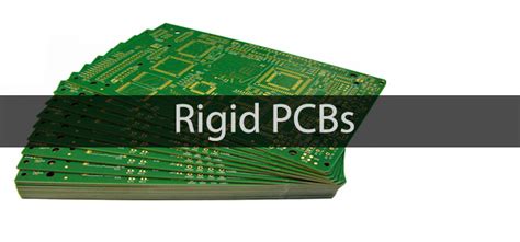
Rigid PCB
What is a Rigid PCB?
A rigid PCB is a type of printed circuit board that uses a solid, non-flexible substrate material such as FR-4 (a glass-reinforced epoxy laminate). Rigid PCBs are the most common type of PCB and are used in a wide range of electronic devices.
Manufacturing Process
The manufacturing process for rigid PCBs is similar to that of other PCB types, depending on the number of layers and the complexity of the circuit.
Applications
Rigid PCBs are used in virtually every electronic device, from simple consumer electronics to complex industrial equipment.
Advantages and Disadvantages
Advantages:
– Excellent mechanical strength and durability
– Suitable for high-density layouts
– Good thermal stability
– Wide range of substrate materials available
Disadvantages:
– Not suitable for applications that require flexibility
– More expensive than flexible PCBs
– Limited shape options
Flexible PCB
What is a Flexible PCB?
A flexible PCB, also known as a flex PCB, is a type of printed circuit board that uses a flexible substrate material such as polyimide or polyester. Flex PCBs can be bent, twisted, and folded to fit into tight spaces or conform to the shape of the device.
Manufacturing Process
The manufacturing process for flex PCBs is similar to that of rigid PCBs, with a few additional steps:
- Designing the PCB layout using a CAD software
- Printing the design onto a photoresist film
- Laminating the photoresist film onto a flexible copper-clad substrate
- Exposing the substrate to UV light to harden the photoresist
- Developing the substrate to remove the unhardened photoresist
- Etching the substrate to remove the unwanted copper
- Applying a cover layer to protect the circuits
- Cutting the substrate to the desired shape
- Testing and inspecting the board
Applications
Flex PCBs are commonly used in applications that require flexibility or space savings, such as:
- Wearable electronics
- Medical devices
- Automotive electronics
- Aerospace equipment
- Portable devices
Advantages and Disadvantages
Advantages:
– Flexibility and conformability
– Space savings
– Lightweight
– Vibration and shock resistance
Disadvantages:
– More expensive than rigid PCBs
– Limited substrate options
– Reduced thermal conductivity
– More complex manufacturing process
Rigid-Flex PCB
What is a Rigid-Flex PCB?
A rigid-flex PCB is a type of printed circuit board that combines the benefits of both rigid and flexible PCBs. Rigid-flex PCBs consist of rigid PCB sections connected by flexible PCB sections, allowing the board to be bent or folded while maintaining the strength and durability of a rigid PCB.
Manufacturing Process
The manufacturing process for rigid-flex PCBs is complex and involves several steps:
- Designing the PCB layout using a CAD software
- Fabricating the rigid and flexible PCB sections separately
- Laminating the rigid and flexible sections together
- Drilling holes for through-hole components and vias
- Plating the holes to create electrical connections between the layers
- Applying a solder mask and silkscreen
- Cutting the board to the desired shape
- Testing and inspecting the board
Applications
Rigid-flex PCBs are commonly used in applications that require both flexibility and strength, such as:
- Aerospace electronics
- Military equipment
- Medical devices
- Automotive electronics
- Portable devices
Advantages and Disadvantages
Advantages:
– Combines the benefits of rigid and flexible PCBs
– Space savings
– Reduced assembly time and costs
– Improved reliability and durability
Disadvantages:
– High cost
– Complex manufacturing process
– Requires specialized design skills
– Longer lead times
High-Frequency PCB
What is a High-Frequency PCB?
A high-frequency PCB is a type of printed circuit board that is designed to handle high-frequency signals (typically above 1 GHz). High-frequency PCBs require special design considerations to minimize signal loss, distortion, and interference.
Manufacturing Process
The manufacturing process for high-frequency PCBs is similar to that of other PCB types, with a few additional considerations:
- Designing the PCB layout using a CAD software with high-frequency simulation tools
- Selecting appropriate substrate materials with low dielectric loss and stable dielectric constant
- Using thinner copper layers to minimize skin effect losses
- Implementing controlled impedance techniques to match trace impedances
- Applying special surface finishes such as immersion silver or electroless nickel/immersion gold (ENIG)
Applications
High-frequency PCBs are commonly used in applications that involve high-speed digital signals or radio frequency (RF) signals, such as:
- Wireless communication devices
- Radar systems
- Satellite equipment
- High-speed digital circuits
- Test and measurement equipment
Advantages and Disadvantages
Advantages:
– Enables high-speed and high-frequency signal transmission
– Reduces signal loss and distortion
– Improves signal integrity and reliability
Disadvantages:
– High cost
– Complex design and manufacturing process
– Requires specialized substrate materials and surface finishes
– Sensitive to manufacturing tolerances and environmental factors
Aluminum PCB
What is an Aluminum PCB?
An aluminum PCB, also known as a metal core PCB (MCPCB), is a type of printed circuit board that uses an aluminum substrate instead of the traditional FR-4 substrate. Aluminum PCBs are designed to provide better thermal management and heat dissipation compared to standard PCBs.
Manufacturing Process
The manufacturing process for aluminum PCBs is similar to that of other PCB types, with a few additional steps:
- Designing the PCB layout using a CAD software with thermal simulation tools
- Applying a dielectric layer to the aluminum substrate to insulate the circuits
- Laminating a copper foil to the dielectric layer
- Etching the copper foil to create the circuit patterns
- Drilling holes for through-hole components and vias
- Applying a solder mask and silkscreen
- Cutting the board to the desired shape
- Testing and inspecting the board
Applications
Aluminum PCBs are commonly used in applications that generate significant amounts of heat, such as:
- Power electronics
- LED lighting
- Automotive electronics
- High-power amplifiers
- Motor drives
Advantages and Disadvantages
Advantages:
– Excellent thermal conductivity and heat dissipation
– Improved reliability and lifespan of electronic components
– Reduced size and weight compared to standard PCBs with heatsinks
– Suitable for high-power applications
Disadvantages:
– Higher cost than standard PCBs
– Limited flexibility in design and layout
– Requires specialized manufacturing processes and equipment
– Potential for thermal expansion mismatch between components and substrate
Types of PCB – FAQ
1. What are the most common types of PCBs?
The most common types of PCBs are single-sided, double-sided, and multi-layer PCBs. These PCBs are widely used in a variety of electronic devices, from simple consumer electronics to complex industrial equipment.
2. What is the difference between a rigid PCB and a flexible PCB?
The main difference between a rigid PCB and a flexible PCB is the substrate material. Rigid PCBs use a solid, non-flexible substrate such as FR-4, while flexible PCBs use a flexible substrate material such as polyimide or polyester. Flexible PCBs can be bent, twisted, and folded to fit into tight spaces or conform to the shape of the device.
3. What are the advantages of using a multi-layer PCB?
Multi-layer PCBs offer several advantages over single-sided and double-sided PCBs, including:
- Higher component density
- Improved signal integrity
- Reduced electromagnetic interference (EMI)
- Suitability for high-speed and high-frequency applications
4. What is a high-frequency PCB, and when is it used?
A high-frequency PCB is a type of printed circuit board designed to handle high-frequency signals (typically above 1 GHz). High-frequency PCBs are used in applications that involve high-speed digital signals or radio frequency (RF) signals, such as wireless communication devices, radar systems, and satellite equipment.
5. What are the benefits of using an aluminum PCB?
Aluminum PCBs, also known as metal core PCBs (MCPCBs), offer several benefits over standard PCBs, including:
- Excellent thermal conductivity and heat dissipation
- Improved reliability and lifespan of electronic components
- Reduced size and weight compared to standard PCBs with heatsinks
- Suitability for high-power applications
| PCB Type | Layers | Flexibility | Thermal Management | Common Applications |
|---|---|---|---|---|
| Single-Sided | 1 | Rigid | Poor | Simple consumer electronics |
| Double-Sided | 2 | Rigid | Poor | Moderately complex devices |
| Multi-Layer | 4+ | Rigid | Moderate | Complex devices, high-speed applications |
| Rigid | Varies | Rigid | Moderate | Wide range of electronic devices |
| Flexible | Varies | Flexible | Poor | Wearable electronics, medical devices |
| Rigid-Flex | Varies | Flexible sections | Moderate | Aerospace, military, portable devices |
| High-Frequency | Varies | Rigid | Moderate | Wireless communication, radar, satellite |
| Aluminum (MCPCB) | Varies | Rigid | Excellent | Power electronics, LED lighting |
Conclusion
Printed Circuit Boards (PCBs) are essential components in modern electronics, providing a reliable and efficient way to interconnect electronic components. There are several types of PCBs, each with its own unique characteristics, manufacturing processes, and applications.
Single-sided, double-sided, and multi-layer PCBs are the most common types, used in a wide range of electronic devices. Rigid PCBs offer excellent mechanical strength and durability, while flexible PCBs provide flexibility and space savings. Rigid-flex PCBs combine the benefits of both rigid and flexible PCBs.
High-frequency PCBs are designed to handle high-frequency signals and are used in applications such as wireless communication and radar systems. Aluminum PCBs, or metal core PCBs, offer superior thermal management and are suitable for high-power applications.
When selecting a PCB type for a specific application, it is essential to consider factors such as the complexity of the circuit, space constraints, thermal management requirements, and signal integrity. By understanding the various types of PCBs and their characteristics, designers and engineers can make informed decisions to create reliable, efficient, and high-performance electronic devices.


Leave a Reply