Introduction to the TL494
The TL494 is a versatile pulse width modulation (PWM) control circuit that is widely used in power supply applications. It is designed to provide all the necessary features for building a high-performance power supply, including voltage and current control, undervoltage lockout, and output protection. In this comprehensive guide, we will cover everything you need to know about the TL494 to help you integrate it into your project successfully.
Key Features of the TL494
The TL494 offers a range of features that make it an ideal choice for power supply applications. Some of the key features include:
- Wide supply voltage range (7V to 40V)
- Adjustable oscillator frequency (1kHz to 300kHz)
- Dual error amplifiers for voltage and current control
- Undervoltage lockout protection
- Output short-circuit protection
- Deadtime control for push-pull outputs
- Pulse-by-pulse current limiting
These features provide designers with the flexibility to customize the TL494 to meet their specific application requirements.

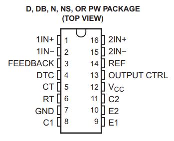
TL494 Pin Configuration and Functions
To effectively use the TL494 in your project, it is essential to understand its pin configuration and the function of each pin. The TL494 is available in a 16-pin DIP or SOIC package. The following table provides a brief description of each pin:
| Pin Number | Pin Name | Description |
|---|---|---|
| 1 | 1IN+ | Non-inverting input of error amplifier 1 |
| 2 | 1IN- | Inverting input of error amplifier 1 |
| 3 | FB | Output of error amplifier 1 |
| 4 | DTC | Deadtime control input |
| 5 | CT | Oscillator timing capacitor |
| 6 | RT | Oscillator timing resistor |
| 7 | GND | Ground |
| 8 | C1 | Collector of output transistor 1 |
| 9 | E1 | Emitter of output transistor 1 |
| 10 | E2 | Emitter of output transistor 2 |
| 11 | C2 | Collector of output transistor 2 |
| 12 | VCC | Positive supply voltage |
| 13 | OUT CTRL | Output control input |
| 14 | 2IN- | Inverting input of error amplifier 2 |
| 15 | 2IN+ | Non-inverting input of error amplifier 2 |
| 16 | REF | 5V reference voltage output |

TL494 Block Diagram and Internal Architecture
To better understand how the TL494 works, it is helpful to examine its internal architecture. The following block diagram illustrates the main components of the TL494:
[Insert TL494 block diagram image here]
The TL494 consists of several key blocks:
- Oscillator: Generates the PWM switching frequency, which can be adjusted using external timing components (RT and CT).
- Error Amplifiers: Two error amplifiers (EA1 and EA2) are used for voltage and current control. They compare the feedback signals with the reference voltage and generate error signals.
- Comparators: The error signals from the amplifiers are fed into comparators, which compare them with the oscillator’s sawtooth waveform to generate PWM signals.
- Output Stage: The PWM signals drive the output transistors (Q1 and Q2) in a push-pull configuration. Deadtime control is provided to prevent shoot-through currents.
- Reference Voltage: The TL494 includes a built-in 5V reference voltage (VREF) that can be used for setting the desired output voltage.
- Protection Circuits: Undervoltage lockout (UVLO) and output short-circuit protection are built into the TL494 to ensure safe operation.

TL494 Application Circuits and Design Considerations
The TL494 can be used in a variety of power supply topologies, including:
- Flyback Converters
- Forward converters
- Push-pull converters
- Half-bridge converters
- Full-bridge converters
When designing a power supply using the TL494, there are several key considerations to keep in mind:
- Oscillator Frequency: Choose the appropriate oscillator frequency based on your application requirements. Higher frequencies allow for smaller transformers and output capacitors but increase switching losses.
- Error Amplifier Compensation: Properly compensate the error amplifiers to ensure stable operation and good transient response. Use the appropriate feedback network and compensation components.
- Output Stage Configuration: Select the appropriate output stage configuration (push-pull, half-bridge, or full-bridge) based on your power requirements and design constraints.
- Transformer Design: Design the power transformer to meet your voltage and current requirements while minimizing leakage inductance and winding capacitance.
- Output Filtering: Use appropriate output filtering (inductors and capacitors) to reduce ripple and noise on the output voltage.
- Protection Circuits: Implement necessary protection circuits, such as overcurrent protection, overvoltage protection, and thermal shutdown, to ensure safe and reliable operation.
TL494 PCB Layout Guidelines
Proper PCB layout is crucial for achieving optimal performance and minimizing noise in your TL494-based power supply. Follow these guidelines when designing your PCB:
- Keep high-current traces short and wide to minimize resistive losses and inductance.
- Separate power ground and signal ground to prevent noise coupling.
- Place the TL494 close to the power transformer and output stage components to minimize trace lengths.
- Use ground planes to provide a low-impedance return path for high-frequency currents.
- Keep sensitive analog traces away from noisy digital traces and power traces.
- Use appropriate bypassing capacitors near the TL494 supply pin to decouple noise.
- Consider using a Faraday shield on the transformer to reduce EMI and improve safety.
TL494 Troubleshooting Tips
If you encounter issues with your TL494-based power supply, here are some troubleshooting tips to help you identify and resolve the problem:
- Check the supply voltage: Ensure that the TL494 is receiving the correct supply voltage (7V to 40V) and that it is within the specified range.
- Verify the oscillator frequency: Use an oscilloscope to measure the oscillator frequency and ensure it matches your design calculations.
- Check the feedback network: Verify that the feedback network is properly connected and that the components are of the correct value.
- Inspect the output waveform: Use an oscilloscope to observe the output waveform and check for any distortion, ringing, or abnormalities.
- Verify the output voltage and current: Measure the output voltage and current to ensure they are within the expected range and meet your design requirements.
- Check for overheating: Monitor the temperature of the TL494 and other components to ensure they are not overheating due to excessive power dissipation or inadequate cooling.
If the issue persists, consult the TL494 datasheet and application notes for further guidance, or seek assistance from experienced power electronics engineers.
Frequently Asked Questions (FAQ)
-
What is the maximum switching frequency of the TL494?
The TL494 can operate at switching frequencies up to 300kHz, making it suitable for a wide range of power supply applications. -
Can the TL494 be used for current-mode control?
Yes, the TL494 can be configured for current-mode control by using one of the error amplifiers for current sensing and feedback. -
How do I set the output voltage of a TL494-based power supply?
The output voltage is set by selecting the appropriate feedback resistors that divide the output voltage and compare it with the internal reference voltage (VREF) of the TL494. -
What is the purpose of the deadtime control (DTC) pin on the TL494?
The deadtime control pin allows you to adjust the deadtime between the switching of the output transistors, preventing shoot-through currents and improving efficiency. -
Can the TL494 be used in parallel for higher power output?
Yes, multiple TL494 ICs can be connected in parallel to increase the output power capability. However, proper current sharing and synchronization techniques must be employed to ensure stable operation.
Conclusion
The TL494 is a powerful and versatile PWM control circuit that finds extensive use in power supply applications. By understanding its features, pin configuration, internal architecture, and application considerations, you can effectively integrate the TL494 into your project and design reliable and efficient power supplies. Remember to follow best practices for PCB layout and troubleshooting to ensure optimal performance and long-term reliability. With the knowledge gained from this comprehensive guide, you are well-equipped to tackle your next power supply project using the TL494.


Leave a Reply