Understanding Component Tombstoning
Component tombstoning is a phenomenon that occurs in electronic circuits when one or more components suddenly fail or become non-functional. This can lead to a variety of issues, such as reduced performance, intermittent operation, or complete failure of the device. In this article, we will explore the causes of component tombstoning, how to identify it, and strategies for preventing it in your designs.
What is Component Tombstoning?
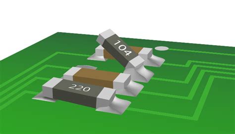
Component tombstoning, also known as “manhattan effect,” “drawbridging,” or “chickenstoning,” is a manufacturing defect that occurs during the surface mount assembly process. It is characterized by one end of a component lifting off the printed circuit board (PCB) pad, while the other end remains attached. This results in the component standing up on one end, resembling a tombstone or a drawbridge.
Tombstoning can affect various types of surface mount components, including:
- Resistors
- Capacitors
- Inductors
- Diodes
- Integrated circuits
When a component tombstones, it creates an open circuit, preventing the flow of electrical current and causing the device to malfunction.
Causes of Component Tombstoning
Several factors can contribute to component tombstoning during the surface mount assembly process:
-
Uneven heating: If one side of a component heats up faster than the other, the solder on the hotter side will melt first, causing the component to lift off the pad on the cooler side.
-
Imbalanced solder paste: Inconsistent or insufficient solder paste application on one pad can lead to uneven solder joint formation, increasing the risk of tombstoning.
-
Component placement issues: Misaligned or poorly centered components can cause one end to have less contact with the solder paste, resulting in a weaker joint that is more prone to tombstoning.
-
PCB Design Factors: Inadequate pad size, incorrect pad spacing, or uneven copper distribution can contribute to tombstoning by affecting the solder joint formation.
-
Reflow profile: An improper reflow profile, such as excessive peak temperature or insufficient time above liquidus, can cause uneven heating and increase the likelihood of tombstoning.
Identifying Component Tombstoning
Identifying component tombstoning is crucial for ensuring the quality and reliability of electronic devices. Here are some methods for detecting tombstoned components:
Visual Inspection
One of the most straightforward ways to identify tombstoned components is through visual inspection. This can be done with the naked eye or using magnification tools such as a microscope or digital microscope. Look for components that are standing up on one end or have a visible gap between the component and the PCB pad.
X-Ray Inspection
X-ray inspection is a non-destructive method for detecting tombstoned components, especially in cases where visual inspection is not possible due to the component’s location or the presence of conformal coating. X-ray images can reveal the internal structure of solder joints and highlight any irregularities or gaps indicative of tombstoning.
Electrical Testing
Functional testing of the assembled PCB can help identify tombstoned components by revealing open circuits or intermittent connections. Techniques such as in-circuit testing (ICT), flying probe testing, or boundary scan testing can be employed to detect tombstoning-related faults.

Preventing Component Tombstoning
To minimize the occurrence of component tombstoning in your designs, consider the following strategies:
Optimize PCB Design
- Ensure that pad sizes are appropriate for the component size and type
- Maintain consistent pad spacing and copper distribution
- Use solder thieves or thermal relief patterns to promote even heating
Improve Solder Paste Application
- Use stencils with the correct aperture size and shape for consistent solder paste deposition
- Regularly maintain and calibrate solder paste printing equipment
- Implement solder paste inspection (SPI) to verify paste volume and placement accuracy
Enhance Component Placement
- Use vision systems or other alignment tools to ensure accurate component placement
- Implement pick-and-place machines with high placement accuracy and repeatability
- Verify Component Orientation and polarity before placement
Optimize Reflow Profile
- Develop a reflow profile that ensures even heating across the PCB
- Maintain adequate time above liquidus (TAL) for proper solder joint formation
- Control the peak temperature and cooling rate to minimize thermal stress
Component Selection
- Choose components with balanced terminations to promote even heating
- Consider using components with longer terminations or wider pitch to reduce tombstoning risk
- Evaluate alternative component packages or sizes that may be less prone to tombstoning

Tombstoning Mitigation Techniques
In some cases, tombstoning may still occur despite preventive measures. Here are some techniques for mitigating the impact of tombstoned components:
Manual Rework
For low-volume production or prototyping, manual rework can be an option for correcting tombstoned components. This involves using a soldering iron to reflow the affected solder joint and reposition the component. However, manual rework can be time-consuming and may introduce other defects if not performed carefully.
Selective Soldering
Selective soldering is an automated process that targets specific components or areas on the PCB for rework. It uses a localized heating source, such as a laser or mini-wave, to reflow the solder joint and allow the component to settle back onto the pad. Selective soldering can be an efficient solution for correcting tombstoned components in high-volume production.
Component Replacement
In some cases, the tombstoned component may be damaged beyond repair, necessitating replacement. This involves removing the defective component and soldering a new one in its place. Component replacement can be done manually or using automated equipment, depending on the production volume and available resources.

Frequently Asked Questions (FAQ)
-
Q: Can tombstoning occur with through-hole components?
A: No, tombstoning is a defect specific to surface mount components. Through-hole components are inserted into holes in the PCB and soldered in place, making them less susceptible to lifting off the pads. -
Q: Is tombstoning more common with certain component sizes?
A: Yes, smaller components with closely spaced terminations, such as chip resistors and capacitors, are more prone to tombstoning due to their lower mass and greater sensitivity to uneven heating. -
Q: Can tombstoning be detected by automated optical inspection (AOI)?
A: Yes, AOI systems can detect tombstoned components by analyzing the height and alignment of components relative to the PCB surface. However, the effectiveness of AOI depends on factors such as camera resolution, lighting, and component orientation. -
Q: How does the solder paste formulation affect tombstoning?
A: The solder paste formulation, particularly the flux and alloy composition, can influence tombstoning. Some solder pastes are formulated to have a wider process window, better wetting properties, or reduced surface tension, which can help minimize tombstoning risk. -
Q: Are there any industry standards or guidelines for preventing tombstoning?
A: Yes, several industry standards and guidelines address tombstoning prevention, such as IPC-A-610 (Acceptability of Electronic Assemblies), IPC-7351 (Generic Requirements for Surface Mount Design and Land Pattern Standard), and IPC-7093 (Design and Assembly Process Implementation for Bottom Termination Components). These standards provide recommendations for PCB design, component selection, and assembly processes to minimize tombstoning and other defects.
| Component Type | Tombstoning Risk | Key Factors |
|---|---|---|
| Chip Resistors | High | – Small size – Closely spaced terminations – Low mass |
| Chip Capacitors | High | – Small size – Closely spaced terminations – Low mass |
| SOT-23 Packages | Moderate | – Asymmetric terminations – Uneven heating |
| QFN Packages | Low | – Large Thermal Pad – Symmetric terminations |
| BGA Packages | Low | – Large number of solder balls – Uniform heating |
Conclusion
Component tombstoning is a common manufacturing defect that can significantly impact the quality and reliability of electronic devices. By understanding the causes of tombstoning and implementing preventive measures in PCB design, solder paste application, component placement, and reflow profile optimization, designers and manufacturers can minimize the occurrence of this issue.
Regular inspection and testing, along with appropriate rework techniques, can help identify and correct tombstoned components, ensuring the proper functioning of the final product. Keeping up with industry standards and best practices is essential for staying ahead of tombstoning challenges and producing high-quality electronic assemblies.


Leave a Reply