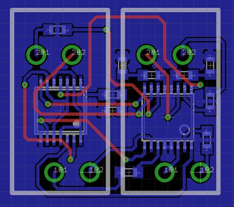
What is PCB Layout?
PCB layout, also known as printed circuit board layout, is the process of designing the physical layout of the components and connections on a PCB. It involves determining the optimal placement of components, routing the electrical connections between them, and ensuring the PCB meets all the necessary electrical, mechanical, and manufacturing requirements.
PCB layout is a critical step in the PCB design process, as it directly impacts the performance, reliability, and manufacturability of the final product. A well-designed PCB layout can minimize signal integrity issues, reduce electromagnetic interference (EMI), improve thermal management, and facilitate efficient manufacturing.
Key Considerations in PCB Layout Design
When designing a PCB layout, several key factors must be considered to ensure the best possible performance and manufacturability:
1. Component Placement
Component placement is one of the most important aspects of PCB layout. The goal is to arrange the components in a way that minimizes the length of electrical connections, reduces signal interference, and facilitates efficient assembly.
Some key considerations for component placement include:
- Grouping related components together
- Placing sensitive components away from sources of interference
- Orienting components to minimize the length of critical signal paths
- Ensuring adequate spacing between components for assembly and maintenance
Component Placement Techniques
| Technique | Description |
|---|---|
| Functional Grouping | Grouping components based on their functional relationships |
| Thermal Grouping | Placing heat-generating components together and away from sensitive components |
| Orientation | Orienting components to minimize the length of critical signal paths and facilitate routing |
| Spacing | Ensuring adequate spacing between components for assembly and maintenance |
2. Signal Routing
Signal routing involves creating the electrical connections between components on the PCB. The goal is to route the signals in a way that minimizes signal integrity issues, such as crosstalk, reflections, and EMI.
Some key considerations for signal routing include:
- Minimizing the length of critical signal paths
- Avoiding sharp bends and vias in high-speed signal traces
- Using appropriate trace widths and spacing for the signal frequency and current
- Implementing proper termination and impedance matching techniques
Common Signal Routing Techniques
| Technique | Description |
|---|---|
| Microstrip | A signal trace on the outer layer of the PCB, with a ground plane on the adjacent layer |
| Stripline | A signal trace embedded between two ground planes within the PCB |
| Coplanar Waveguide | A signal trace with ground planes on either side on the same layer |
| Differential Pairs | Two signal traces routed together with a specific spacing and impedance to carry differential signals |
3. Power Distribution
Power distribution is the process of delivering power to the components on the PCB. The goal is to provide a stable and noise-free power supply to all components while minimizing voltage drops and power losses.
Some key considerations for power distribution include:
- Using appropriate trace widths and copper thicknesses for the expected current
- Placing power and ground planes on adjacent layers to minimize inductance
- Implementing proper decoupling and filtering techniques to reduce power supply noise
- Using separate power supplies or regulators for noise-sensitive components
Power Distribution Network (PDN) Design
A well-designed PDN is essential for ensuring a stable and noise-free power supply to all components on the PCB. Some key elements of a PDN include:
- Power and ground planes
- Decoupling capacitors
- Voltage regulators
- Power connectors and distribution traces
4. Grounding and Shielding
Proper grounding and shielding techniques are essential for minimizing EMI and ensuring signal integrity in a PCB layout.
Some key considerations for grounding and shielding include:
- Using a solid ground plane to provide a low-impedance return path for signals
- Implementing a star grounding scheme to minimize ground loops and noise
- Using shielding techniques, such as grounded copper pours or metal enclosures, to reduce EMI
- Separating analog and digital grounds to minimize noise coupling
Grounding Techniques
| Technique | Description |
|---|---|
| Solid Ground Plane | A continuous layer of copper on a PCB layer dedicated to ground |
| Star Grounding | A grounding scheme where all ground connections meet at a single point to minimize ground loops |
| Hybrid Grounding | A combination of solid ground plane and star grounding techniques |
| Analog and Digital Ground Separation | Separating analog and digital ground planes to minimize noise coupling |
5. Thermal Management
Thermal management is the process of dissipating heat generated by components on the PCB to prevent overheating and ensure reliable operation.
Some key considerations for thermal management include:
- Placing heat-generating components away from temperature-sensitive components
- Using appropriate copper pours and thermal vias to dissipate heat
- Implementing thermal interface materials, such as thermal pads or adhesives, to improve heat transfer
- Considering the use of heatsinks or fans for high-power components
Thermal Management Techniques
| Technique | Description |
|---|---|
| Copper Pours | Large areas of copper on the PCB layers used to dissipate heat |
| Thermal Vias | Vias filled with thermally conductive material to transfer heat between layers |
| Thermal Interface Materials | Materials, such as thermal pads or adhesives, used to improve heat transfer between components and the PCB |
| Heatsinks and Fans | External components used to dissipate heat from high-power components |

PCB Layout Design Process
The PCB layout design process typically involves the following steps:
-
Schematic Review: Review the schematic to ensure it is complete, accurate, and meets the design requirements.
-
Component Placement: Place the components on the PCB, considering factors such as functional grouping, thermal management, and signal routing.
-
Signal Routing: Route the electrical connections between components, considering factors such as signal integrity, EMI, and manufacturability.
-
Power Distribution: Design the power distribution network, including power and ground planes, decoupling capacitors, and voltage regulators.
-
Grounding and Shielding: Implement grounding and shielding techniques to minimize EMI and ensure signal integrity.
-
Thermal Management: Incorporate thermal management techniques, such as copper pours and thermal vias, to dissipate heat from components.
-
Design Rule Check (DRC): Perform a DRC to ensure the PCB layout meets the manufacturing and design requirements.
-
Documentation: Generate the necessary documentation, such as assembly drawings and bill of materials (BOM), for manufacturing and assembly.

Best Practices for PCB Layout Design
To ensure a successful PCB layout design, consider the following best practices:
-
Start with a Good Schematic: Ensure the schematic is complete, accurate, and well-organized before starting the PCB layout.
-
Plan the Layout: Plan the overall layout, including component placement and signal routing, before starting the detailed design.
-
Use a Hierarchical Design Approach: Break the design into smaller, more manageable sections and work on them individually.
-
Keep Signal Paths Short: Minimize the length of critical signal paths to reduce signal integrity issues and improve performance.
-
Minimize Crosstalk: Use appropriate spacing and shielding techniques to minimize crosstalk between signals.
-
Use a Solid Ground Plane: Use a solid ground plane to provide a low-impedance return path for signals and minimize EMI.
-
Decouple Power Supplies: Use decoupling capacitors to reduce power supply noise and ensure a stable power supply to components.
-
Consider Manufacturability: Design the PCB with manufacturing in mind, considering factors such as minimum trace widths, spacings, and hole sizes.
-
Document the Design: Provide clear and comprehensive documentation, including assembly drawings and BOMs, to facilitate manufacturing and assembly.
-
Collaborate with Manufacturers: Work closely with PCB manufacturers and assembly houses to ensure the design is manufacturable and meets their requirements.

Frequently Asked Questions (FAQ)
1. What is the difference between a schematic and a PCB layout?
A schematic is a graphical representation of the electrical connections and components in a circuit, while a PCB layout is the physical arrangement of those components and connections on a printed circuit board.
2. What are the main factors to consider when placing components on a PCB?
The main factors to consider when placing components on a PCB include functional grouping, thermal management, signal routing, and manufacturability.
3. What is the purpose of a ground plane in a PCB layout?
The purpose of a ground plane in a PCB layout is to provide a low-impedance return path for signals, minimize EMI, and ensure a stable reference voltage for components.
4. What are some common signal integrity issues in PCB layouts?
Some common signal integrity issues in PCB layouts include crosstalk, reflections, ground bounce, and EMI.
5. How can thermal management be addressed in a PCB layout?
Thermal management in a PCB layout can be addressed through techniques such as placing heat-generating components away from temperature-sensitive components, using copper pours and thermal vias to dissipate heat, and implementing thermal interface materials or heatsinks for high-power components.
Conclusion
PCB layout design is a critical step in the PCB design process, directly impacting the performance, reliability, and manufacturability of the final product. By considering key factors such as component placement, signal routing, power distribution, grounding and shielding, and thermal management, and following best practices and collaborating with manufacturers, designers can create PCB layouts that meet the necessary requirements and ensure a successful product.


Leave a Reply