What is PCB Assembly?
PCB Assembly, short for Printed Circuit Board Assembly, is the process of attaching electronic components to a printed circuit board to create a functional electronic device. The process involves several steps, including placing components on the board, soldering them in place, and testing the finished assembly to ensure proper functionality.
The Importance of PCB Assembly
PCB Assembly is a crucial step in the manufacturing of electronic devices. It allows for the creation of complex circuits in a compact and efficient manner, enabling the production of a wide range of electronic products, from smartphones and laptops to medical devices and aerospace equipment.
The PCB Assembly Process
The PCB Assembly process typically involves the following steps:
- Solder Paste Application
- Component Placement
- Reflow Soldering
- Inspection and Testing
1. Solder Paste Application
The first step in the PCB Assembly process is applying solder paste to the PCB. Solder paste is a mixture of tiny solder particles and flux, which helps the solder adhere to the PCB and components. There are two main methods for applying solder paste:
Stencil Printing
Stencil printing involves using a stencil with openings that correspond to the pads on the PCB. The solder paste is applied over the stencil, and a squeegee is used to spread the paste evenly across the openings. This method is fast and accurate, making it suitable for high-volume production.
Jet Printing
Jet printing uses a specialized printer to dispense solder paste directly onto the PCB pads. This method is slower than stencil printing but offers more flexibility and is suitable for prototyping and low-volume production.
2. Component Placement
Once the solder paste has been applied, the next step is to place the components onto the PCB. There are two main methods for component placement:
Manual Placement
Manual placement involves using tweezers or a pick-and-place machine to place components onto the PCB by hand. This method is suitable for low-volume production or prototyping but is time-consuming and prone to human error.
Automated Placement
Automated placement uses a machine to pick and place components onto the PCB. These machines are programmable and can place components with high speed and accuracy, making them suitable for high-volume production.
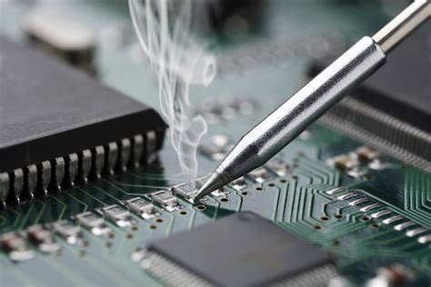
3. Reflow Soldering
After the components have been placed, the PCB is ready for soldering. Reflow soldering involves heating the PCB and components to melt the solder paste and create a permanent connection. There are two main types of reflow soldering:
Convection Reflow
Convection reflow uses hot air to heat the PCB and components. The PCB is placed in an oven, and hot air is circulated around it to melt the solder paste. This method is suitable for most PCB assemblies and is widely used in the industry.
Vapor Phase Reflow
Vapor phase reflow uses a specialized fluid to heat the PCB and components. The PCB is placed in a chamber filled with the fluid, which boils and creates a vapor that envelops the PCB, heating it evenly. This method offers more precise temperature control and is suitable for assemblies with heat-sensitive components.
4. Inspection and Testing
After the soldering process, the PCB assembly undergoes inspection and testing to ensure proper functionality. There are several methods for inspection and testing:
Visual Inspection
Visual inspection involves examining the PCB assembly under a microscope or magnifying glass to check for defects such as solder bridges, misaligned components, or incomplete solder joints.
Automated Optical Inspection (AOI)
AOI uses cameras and image processing software to automatically inspect the PCB assembly for defects. This method is fast and accurate, making it suitable for high-volume production.
X-Ray Inspection
X-ray inspection uses X-rays to examine the internal structure of the PCB assembly, allowing for the detection of defects that may not be visible on the surface.
Functional Testing
Functional testing involves powering up the PCB assembly and testing its functionality to ensure it meets the specified requirements. This may include tests for signal integrity, power consumption, and overall performance.

Types of PCB Assembly
There are two main types of PCB Assembly:
Through-Hole Assembly
Through-hole assembly involves inserting component leads through holes drilled in the PCB and soldering them in place on the opposite side. This method is suitable for larger components and offers a stronger mechanical connection but is slower and more labor-intensive than surface mount assembly.
Surface Mount Assembly
Surface mount assembly involves placing components directly onto pads on the surface of the PCB and soldering them in place. This method is faster and more automated than through-hole assembly and allows for smaller components and higher component density. Surface mount assembly is the most common method used in the industry today.
| Assembly Type | Characteristics | Advantages | Disadvantages |
|---|---|---|---|
| Through-Hole | Components inserted through holes in PCB | Stronger mechanical connection, suitable for larger components | Slower, more labor-intensive |
| Surface Mount | Components placed directly on PCB surface | Faster, more automated, allows for smaller components and higher density | Not as strong mechanically, requires more precise placement |

Choosing a PCB Assembly Service
When selecting a PCB Assembly service, there are several factors to consider:
Experience and Expertise
Choose a service provider with extensive experience and expertise in PCB Assembly, particularly in the type of assembly required for your project (through-hole or surface mount).
Quality Control
Ensure the service provider has robust quality control processes in place, including inspection and testing procedures to guarantee the reliability and functionality of the finished assembly.
Turnaround Time
Consider the service provider’s turnaround time and whether it meets your project timeline. Some providers offer expedited services for time-sensitive projects.
Cost
Compare costs between different service providers, but be cautious of selecting based on price alone. Lower costs may indicate lower quality or less experienced providers.
Customer Support
Look for a service provider with responsive and knowledgeable customer support to assist with any questions or issues that may arise during the assembly process.

Frequently Asked Questions (FAQ)
-
Q: What is the difference between PCB fabrication and PCB assembly?
A: PCB fabrication is the process of manufacturing the bare PCB, while PCB assembly involves attaching components to the fabricated board to create a functional electronic device. -
Q: How long does the PCB assembly process typically take?
A: The turnaround time for PCB assembly varies depending on the complexity of the design and the service provider. Simple assemblies may take a few days, while more complex projects can take several weeks. -
Q: What are the most common defects encountered in PCB assembly?
A: Common defects include solder bridges, cold solder joints, misaligned components, and incomplete solder joints. These defects can be minimized through proper process control and quality inspection. -
Q: Can I assemble my own PCBs?
A: Yes, it is possible to assemble PCBs yourself, particularly for simple designs or prototyping. However, for complex designs or high-volume production, it is usually more efficient and cost-effective to use a professional PCB assembly service. -
Q: What information do I need to provide when ordering PCB assembly services?
A: When ordering PCB assembly services, you will typically need to provide the PCB design files (Gerber files), bill of materials (BOM), and assembly instructions. Some service providers may also require additional information, such as CAD files or test specifications.
Conclusion
PCB Assembly is a critical process in the production of electronic devices, enabling the creation of complex circuits in a compact and efficient manner. By understanding the various steps involved in the assembly process, as well as the different types of assembly and factors to consider when choosing a service provider, you can ensure the successful production of your electronic projects. With the right knowledge and partner, PCB Assembly can help bring your electronic designs to life.


Leave a Reply