Introduction to PCB Panel Size
When it comes to printed circuit board (PCB) manufacturing, one of the most important considerations is the PCB panel size. The panel size refers to the dimensions of the larger board from which individual PCBs are cut out. Choosing the right panel size is crucial for optimizing the manufacturing process, minimizing costs, and ensuring the quality of the final product.
In this comprehensive article, we’ll dive deep into the world of PCB panel sizes, covering everything you need to know to make informed decisions for your PCB projects.
Why PCB Panel Size Matters
The PCB panel size plays a significant role in several aspects of the manufacturing process:
-
Cost-effectiveness: Selecting the optimal panel size allows manufacturers to maximize the number of PCBs produced per panel, reducing material waste and lowering production costs.
-
Manufacturing efficiency: Standardized panel sizes enable the use of automated assembly lines, streamlining the production process and minimizing human error.
-
Quality control: Proper panel sizing ensures that PCBs are cut out accurately, maintaining the integrity of the circuit design and preventing issues such as copper burring or edge defects.
-
Compatibility: Choosing a compatible panel size is essential for seamless integration with the manufacturer’s equipment and processes.

Standard PCB Panel Sizes
To facilitate efficient and cost-effective manufacturing, the PCB industry has established a set of standard panel sizes. These sizes are designed to be compatible with most manufacturing equipment and processes. Some of the most common standard PCB panel sizes include:
| Panel Size (mm) | Panel Size (inches) |
|---|---|
| 100 x 100 | 3.94 x 3.94 |
| 200 x 200 | 7.87 x 7.87 |
| 300 x 300 | 11.81 x 11.81 |
| 400 x 400 | 15.75 x 15.75 |
| 450 x 450 | 17.72 x 17.72 |
It’s important to note that while these are the most common standard sizes, some manufacturers may offer additional options or have specific requirements. Always consult with your chosen manufacturer to ensure compatibility and availability.

Factors Influencing PCB Panel Size Selection
When selecting the appropriate PCB panel size for your project, consider the following factors:
-
PCB dimensions: The dimensions of your individual PCBs will determine the minimum panel size required to accommodate them.
-
Quantity: The number of PCBs you need to produce will influence the panel size selection. Larger quantities may benefit from larger panel sizes to optimize production efficiency.
-
Manufacturing capabilities: Ensure that your chosen panel size is compatible with your manufacturer’s equipment and processes.
-
Material availability: Some panel sizes may be more readily available than others, depending on the material and thickness required for your PCBs.
-
Cost considerations: Larger panel sizes may offer cost savings due to reduced material waste and increased production efficiency. However, this must be balanced against the specific requirements of your project.

Optimizing PCB Layout for Panel Size
To make the most of your chosen PCB panel size, consider the following tips when designing your PCB layout:
-
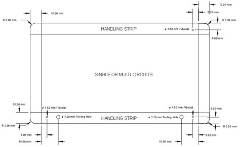
Panelization: Arrange your PCBs on the panel in a way that maximizes the number of boards per panel while leaving sufficient space for tooling holes, fiducial marks, and other necessary features.
-
Spacing: Ensure adequate spacing between individual PCBs to allow for clean and accurate cutting during the depaneling process.
-
Orientation: Consider the orientation of your PCBs on the panel to minimize material waste and optimize the use of available space.
-
Tooling holes: Include appropriate tooling holes in your panel design to facilitate handling and alignment during the manufacturing process.
-
Fiducial marks: Incorporate fiducial marks into your panel layout to aid in the alignment and registration of the PCBs during assembly.
Advanced PCB Panel Techniques
In addition to standard panel sizes, there are several advanced techniques that can be employed to further optimize PCB manufacturing:
-
Step and repeat: This technique involves creating a master panel design that includes multiple copies of the same PCB layout, allowing for efficient mass production.
-
Mixed panels: Mixed panels incorporate different PCB designs on the same panel, enabling the production of multiple PCB variants in a single manufacturing run.
-
Sub-panels: Sub-paneling involves dividing a larger panel into smaller sections, each containing a subset of the total number of PCBs. This technique can be useful for managing larger production runs or accommodating specific manufacturing requirements.
PCB Panelization Software
To streamline the process of designing and optimizing PCB panels, many designers and engineers rely on specialized PCB panelization software. These tools offer features such as:
-
Automatic panelization: Automatically arrange PCBs on the panel based on specified parameters and constraints.
-
Panel optimization: Identify the most efficient panel layout to maximize PCB yield and minimize material waste.
-
Design rule checks: Verify that the panel design adheres to manufacturing guidelines and constraints.
-
Output generation: Generate manufacturing-ready output files, such as Gerber files, drill files, and assembly data.
Some popular PCB panelization software options include:
- PCB Panelizer by Numerical Innovations
- Panel Designer by Ucamco
- PCB Panel Expert by DownStream Technologies
Frequently Asked Questions (FAQ)
1. What happens if I choose a non-standard PCB panel size?
While non-standard panel sizes can be accommodated, they may result in increased manufacturing costs and longer lead times due to the need for custom tooling and setup. It’s always best to consult with your manufacturer to understand their capabilities and limitations.
2. Can I mix different PCB thicknesses on the same panel?
In most cases, it’s not recommended to mix different PCB thicknesses on the same panel, as this can lead to issues with the depaneling process and may require additional handling. If you need to produce PCBs with different thicknesses, it’s best to use separate panels for each thickness.
3. How do I determine the optimal panel size for my project?
To determine the optimal panel size, consider factors such as your individual PCB dimensions, the quantity required, manufacturing capabilities, material availability, and cost considerations. Consult with your manufacturer and use PCB panelization software to identify the most efficient and cost-effective solution.
4. What is the minimum spacing required between PCBs on a panel?
The minimum spacing between PCBs on a panel depends on the specific manufacturing process and equipment used. As a general guideline, a minimum spacing of 2-3 mm is often recommended, but it’s crucial to consult with your manufacturer for their specific requirements.
5. Can I use the same panel design for different PCB fabricators?
While it’s possible to use the same panel design for different PCB fabricators, it’s essential to verify that the design is compatible with each fabricator’s specific requirements and capabilities. Some fabricators may have unique guidelines or constraints that need to be considered in the panel design.
Conclusion
PCB panel size is a critical aspect of PCB manufacturing that directly impacts cost, efficiency, quality, and compatibility. By understanding the standard panel sizes, factors influencing panel size selection, and optimization techniques, you can make informed decisions that streamline your PCB production process.
Remember to collaborate closely with your chosen PCB manufacturer, leverage PCB panelization software, and stay up-to-date with industry best practices to ensure the success of your PCB projects.


Leave a Reply