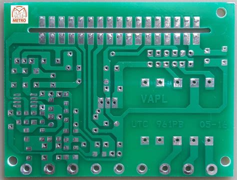
What is a Single-Sided PCB?
A single-sided PCB, also known as a Single-Layer PCB, is a printed circuit board that has conductive traces on only one side of the board. The other side of the board is typically left bare or coated with a solder mask to prevent short circuits. Single-sided PCBs are the simplest and most cost-effective type of PCB, making them a popular choice for low-complexity electronic projects and prototypes.
Advantages of Single-Sided PCBs
- Cost-effective: Single-sided PCBs are the most affordable type of PCB due to their simple design and manufacturing process.
- Easy to design: With only one layer to work with, designing a single-sided PCB is relatively straightforward compared to multi-layer PCBs.
- Quick turnaround: The manufacturing process for single-sided PCBs is faster than that of multi-layer PCBs, resulting in shorter lead times.
- Suitable for low-complexity projects: Single-sided PCBs are ideal for simple electronic projects that do not require a high component density or complex routing.
Disadvantages of Single-Sided PCBs
- Limited routing options: With only one layer available for routing, single-sided PCBs may require more jumper wires or creative routing solutions for more complex designs.
- Lower component density: Single-sided PCBs cannot accommodate as many components as multi-layer PCBs due to the limited space available on one side of the board.
- Reduced electrical performance: Single-sided PCBs may have higher electromagnetic interference (EMI) and signal integrity issues compared to multi-layer PCBs.
How to Design a Single-Sided PCB
Step 1: Choose a PCB Design Software
There are various PCB design software options available, ranging from free, open-source tools to paid, professional-grade software. Some popular choices include:
- KiCad (free and open-source)
- Eagle (free for non-commercial use, paid for commercial use)
- Altium Designer (paid, professional-grade)
- OrCAD (paid, professional-grade)
Step 2: Create a Schematic
Begin by creating a schematic of your electronic circuit. A schematic is a graphical representation of the electrical connections between components in your design. It helps you visualize the circuit and ensures that all components are correctly connected before proceeding to the PCB layout.
Step 3: Create a Component Library
If your chosen PCB design software does not have a built-in library with the components you need, you may need to create your own component library. This involves defining the schematic symbols and footprints for each component in your design.
Step 4: Design the PCB Layout
Once your schematic is complete, you can begin designing the PCB layout. This involves arranging the components on the board and routing the traces between them. When designing a single-sided PCB, keep the following tips in mind:
- Place components strategically to minimize the number of jumper wires needed.
- Use wider traces for power and ground connections to reduce resistance and improve current-carrying capacity.
- Maintain appropriate clearances between traces and components to avoid short circuits and manufacturing issues.
- Use a grid to ensure proper alignment of components and traces.
Step 5: Generate Gerber Files
After completing the PCB layout, generate Gerber files, which are the standard file format used by PCB manufacturers. Gerber files contain all the necessary information for manufacturing your PCB, including the copper layer, solder mask, silkscreen, and drill data.

Single-Sided PCB Manufacturing Process
Step 1: Substrate Preparation
The PCB manufacturing process begins with the preparation of the substrate, which is typically a laminate material such as FR-4. The substrate is cut to the desired size and shape of the PCB.
Step 2: Copper Cladding
A thin layer of copper foil is bonded to one side of the substrate using heat and pressure. The copper layer will form the conductive traces on the PCB.
Step 3: Applying Photoresist
A photosensitive resist is applied to the copper layer. This resist will be used to transfer the PCB layout pattern onto the copper.
Step 4: Exposure and Development
The PCB layout pattern is transferred onto the photoresist using a photolithographic process. The photoresist is exposed to UV light through a photomask, which contains the PCB layout pattern. The exposed areas of the photoresist become soluble and are removed during the development process, leaving the desired pattern on the copper layer.
Step 5: Etching
The exposed copper areas are etched away using a chemical solution, typically ferric chloride or ammonium persulfate. This leaves only the desired copper traces on the PCB.
Step 6: Solder Mask Application (Optional)
A solder mask can be applied to the PCB to protect the copper traces and prevent short circuits. The solder mask is typically green in color and is applied using a silkscreen printing process.
Step 7: Silkscreen Printing (Optional)
A silkscreen layer can be added to the PCB to provide text, logos, or component outlines. This layer is typically white and is applied using a silkscreen printing process.
Step 8: Surface Finish (Optional)
A surface finish can be applied to the exposed copper areas to improve solderability and protect the copper from oxidation. Common surface finishes include HASL (Hot Air Solder Leveling), ENIG (Electroless Nickel Immersion Gold), and OSP (Organic Solderability Preservative).
Step 9: Drilling
Holes are drilled through the PCB to accommodate through-hole components and vias. The drilling process is typically done using a CNC drilling machine.
Step 10: Cutting and Routing
The individual PCBs are cut and routed from the larger panel using a routing machine. This process creates the final shape and size of the PCB.

Cost-Saving Strategies for Single-Sided PCBs
1. Panelize Your Design
Panelizing your PCB design involves arranging multiple copies of your PCB on a single panel. This can help reduce manufacturing costs by minimizing the number of panels required and optimizing material usage. When panelizing your design, consider the following factors:
- Panel size: Choose a panel size that maximizes the number of PCBs per panel while minimizing waste.
- Spacing: Ensure adequate spacing between individual PCBs to allow for cutting and routing.
- Tooling holes: Include tooling holes in the panel design to aid in the manufacturing process.
2. Use Standard Sizes and Shapes
Using standard PCB sizes and shapes can help reduce manufacturing costs by allowing manufacturers to optimize their processes and material usage. Some common standard sizes include:
| Size (mm) | Size (inches) |
|---|---|
| 100 x 100 | 3.94 x 3.94 |
| 150 x 100 | 5.91 x 3.94 |
| 200 x 150 | 7.87 x 5.91 |
| 250 x 200 | 9.84 x 7.87 |
3. Minimize the Number of Drill Sizes
Using fewer drill sizes in your PCB design can help reduce manufacturing costs by simplifying the drilling process and reducing the number of drill bit changes required. When possible, use standard drill sizes and minimize the number of unique drill sizes in your design.
4. Opt for a Smaller Board Size
Choosing a smaller board size can help reduce material costs and manufacturing time. However, be sure to balance board size with component density and routing complexity to ensure that your design is still manufacturable.
5. Consider a Cheaper Surface Finish
While some surface finishes, such as ENIG, offer superior performance and durability, they can also be more expensive. For cost-sensitive projects, consider using a cheaper surface finish, such as HASL or OSP, which can still provide adequate protection and solderability.

FAQ
1. What is the minimum trace width for a single-sided PCB?
The minimum trace width for a single-sided PCB depends on the PCB manufacturer’s capabilities and the specific design requirements. Typically, a minimum trace width of 0.15mm to 0.2mm is achievable for most single-sided PCB designs.
2. Can single-sided PCBs have vias?
Yes, single-sided PCBs can have vias, which are used to connect traces on the same layer. However, single-sided PCBs cannot have plated through-hole vias, which are used to connect traces on different layers in multi-layer PCBs.
3. What is the maximum component density for a single-sided PCB?
The maximum component density for a single-sided PCB depends on various factors, such as the component sizes, routing complexity, and manufacturing capabilities. As a general rule, single-sided PCBs have a lower component density compared to multi-layer PCBs due to the limited routing space available on one side of the board.
4. How much does a single-sided PCB cost compared to a double-sided PCB?
Single-sided PCBs are generally less expensive than double-sided PCBs due to their simpler design and manufacturing process. The exact cost difference depends on factors such as the PCB size, quantity, and manufacturer. On average, a single-sided PCB can cost 20-30% less than a comparable double-sided PCB.
5. Are single-sided PCBs suitable for high-frequency applications?
Single-sided PCBs may not be the best choice for high-frequency applications due to their limited ability to control impedance and higher susceptibility to electromagnetic interference (EMI). For high-frequency applications, multi-layer PCBs with proper grounding and shielding techniques are generally recommended.
Conclusion
Single-sided PCBs offer a cost-effective solution for low-complexity electronic projects and prototypes. By understanding the design considerations, manufacturing process, and cost-saving strategies associated with single-sided PCBs, you can optimize your designs for affordability and manufacturability. While single-sided PCBs may have limitations in terms of routing options and component density, they remain a valuable tool in the electronics industry for simple, cost-sensitive applications.


Leave a Reply