Introduction
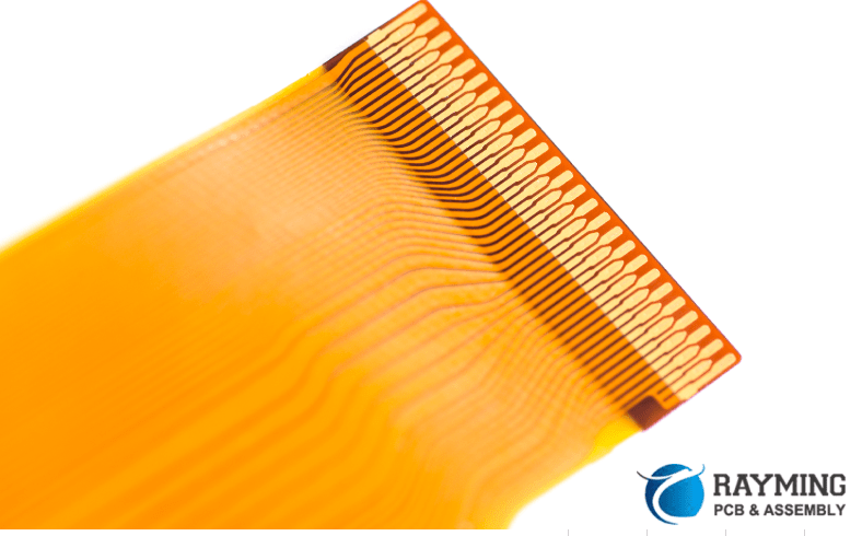
Flexible printed circuit boards (PCBs), also known as flex circuits, are made with flexible substrate materials that can bend and flex without damage. Single layer flex PCBs have a single conductive copper layer on one side of the flex substrate. They provide a simple and cost-effective solution for many electronic applications requiring dynamic flexing, bending or wrapping around surfaces.
In this comprehensive guide, we will cover everything you need to know about single layer flexible PCBs including:
- Benefits and applications
- Flexible substrate materials
- Design considerations
- Manufacturing processes
- Quality testing
- Cost factors
Understanding the capabilities and limitations of single layer flex PCB technology will allow you to determine if it is suitable for your application. We’ll also provide tips for getting the most out of your flexible PCB design while avoiding common mistakes. Let’s get started!
Benefits and Applications of Single Layer Flex Circuits
Flexible PCBs provide a number of advantages over traditional rigid boards:
Dynamic Flexing – The flexible substrate allows for repeated bending and shaping without damage. This makes them ideal for applications where the circuit needs to change shape or adapt to surfaces.
Lightweight – Flex circuits are extremely lightweight and thin. This helps reduce product weight.
Durable – The boards are highly durable against vibration, shock and temperature fluctuations. The laminated construction protects against dust and moisture.
Space savings – Flex boards can fit into tight, compact spaces where rigid boards won’t work.
Production costs – Simple single layer designs reduce layers and processing steps, which lowers costs.
Some common applications that utilize single layer flex PCBs include:
- Wearable devices
- Medical monitors
- Robotics/UAVs
- IO connectors
- Sensors
- Low speed ribbon cables
- Heater elements
For simple low-speed connections, single layer flex provides an affordable option. The flexible nature allows the PCB to adapt to the best path between endpoints. The thin profile is ideal when space constraints are an issue.
Flexible Substrate Materials
The flexible substrate, also called the dielectric, is what gives flex PCBs their distinct bendable properties. While rigid boards use materials like FR-4, flex PCBs use different flexible polymer films and sheets laminated with adhesive.
Some common substrates used include:
Polyimide (PI) – This is the most popular flex substrate. Polyimide offers high flex life, temperature resistance, chemical resistance and dielectric strength. Common brands are Kapton from DuPont and Apical from Kaneka.
Polyester (PET) – Polyester films like Mylar offer very good flex life and dimensional stability at a lower cost than polyimide. The downside is lower temperature rating.
Polyethylene (PE) – Polyethylene terephthalate or PET provides good flexibility and a lower cost option. However, it has lower temperature resistance than other substrates.
Fluoropolymers (PTFE) – PTFE substrates provide temperature resistance up to nearly 300°C. The downside is poorer flex life and higher material costs.
For most single layer flex applications, polyimide or polyester films offer the best balance of properties and cost. The substrate thickness is typically between 25-100μm.
Design Considerations for Single Layer Flex
Designing a reliable single layer flex PCB requires accounting for the dynamics of the flexible substrate. Here are some key considerations:
Bend radius – Avoid tight folds and maintain bend radius above minimum levels. Inside bend radii below 3-5x board thickness can damage traces.
Layer stackup – With only one conductive copper layer, maintain at least 25μm dielectric to prevent pinholes/breakdown.
Conductor width/spacing – Use wider traces and spacing for dynamic flexing to prevent openings or shorts. Minimum 6-8mil width and spacing.
Stiffeners – Add stiffener strips along bend areas or consider selective stiffening with solder mask or laminate layers.
Adhesives – Use flexible acrylic or epoxy adhesives suited for dynamic bending applications.
Vias – Use staggered pad shapes for vias to relieve stress concentrations. Filled and capped vias improve reliability.
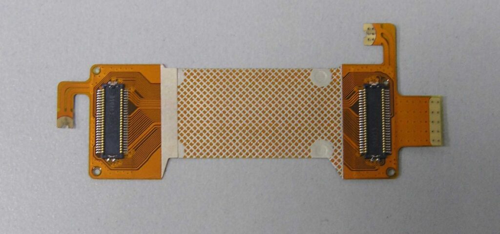
Connections – Reinforce connectors and avoid rigid attachments. Design flex-to-board connections carefully.
Thermal expansion – Account for CTE mismatch between flex board and components. Use compliance design techniques.
Paying attention to these areas will ensure your flex PCB stand up to continuous bending without any reliability issues.
Manufacturing Process for Single Layer Flex Circuits
Producing reliable single layer flex PCBs requires specialized manufacturing processes tailored for flexible circuits. Here is an overview of the typical manufacturing workflow:
1. Design Input – The process starts with receiving the Gerber and drill files for the circuit layout. The design is reviewed to ensure it meets flex board requirements.
2. Photoimageable Processing – Liquid photoimageable (LPI) solder mask, legend, and marking are screen printed or electrodeposited onto the base laminate material. This is exposed to UV then developed to form the protective coating.
3. Etching – The conductive copper layer is chemically etched to form the conductors (traces, pads, vias) according to the layout patterns.
4. Hole Drilling – Mechanical drilling machines with carbide bits drill any through holes for vias or mounting. Flex boards use smaller hole sizes than rigid boards.
5. Connecting – Conductive adhesives or solder paste are applied to connect surface mount components. Reflow or thermal bonding attaches the components.
6. Testing and Inspection – Each board is electrically tested. Parameters like continuity, resistance, and insulation are verified. Automated optical inspection (AOI) checks for defects.
7. Singulation – Individual PCB units are cut or routed from the larger panel. This is usually done with a steel rule die or CO2 laser cutting.
8. Electrical Testing – Additional testing such as flying probe electrical test occurs after final singulation.
9. Final Quality Inspection – Each board undergoes final visual inspection for any flaws. Dimensional tolerances are also checked.
This optimized process ensures quality and reliability for the completed single layer flex circuits.
Quality Testing and Inspection
Thorough testing and inspection at all stages is critical for flexible PCBs:
Dimensional Tolerances – Measure and verify board dimensions, conductor widths, drill holes, and other physical attributes are within specified tolerances.
Bend Radii – Inspect minimum inside bend radius meets the design specification, often 3-5X the board thickness.
Adhesion – Conduct 90 or 180 degree peel tests to check bond strength of laminate and copper adhesive. Minimum values ensure good adhesion.
Flexibility – Test via bend or twist tests to ensure the PCB can flex continuously without cracks or connections breaking.
Electrical – Use flying probe or bed-of-nails testers to verify electrical continuity, resistance, and isolation on boards meet requirements.
Circuit Function – Perform functional testing of the fully assembled board for correct end-to-end operation of the circuit.
Visual – Inspect boards under high magnification for any detectable flaws in traces, connections, or substrate.
By thoroughly verifying each quality parameter, any defects or issues can be identified before the product ships.
Cost Factors
When budgeting for your single layer flex PCB project, here are some of the main cost factors:
- Board size – Although flexible PCBs are priced by area, larger boards spread costs over more units. Allow for material utilization.
- Design complexity – Simple layouts with more spacing will be cheaper than dense, complex ones. Number of drill holes also adds costs.
- Flex vs. rigid – Rigid boards generally cost less at high volumes. But for prototypes and lower volumes, flex can be cheaper.
- Volume – As with any PCB, higher order volumes will provide better pricing. Prototypes cost much more.
- Testing/QC – Adding electrical testing, functional testing, and other quality checks will increase costs.
- Special requirements – Unique materials, quick turnaround times or other requirements will drive increased costs.
Work closely with your flex PCB supplier to identify design choices and process tweaks that can help reduce costs. Taking the time upfront to optimize the design and manufacturability will pay dividends for keeping your program on budget.
FQA
Why choose single layer flex PCBs?
Some reasons to choose single layer flex PCBs:
- Low cost, simple design
- Dynamic or static flexing needed
- Thin, lightweight board required
- Tight spaces or compact device
- Low speed circuitry only
Single layer flex provides a cost-effective option when multilayer boards are overkill.
What are some examples of single layer flex applications?
Typical applications include:
- Wearable devices
- Heaters or sensors requiring bending
- Ribbon cables for bending connections
- IO connectors and small harnesses
- Medical monitoring patches
- Robotics or UAV folding joints
Any application requiring a thin, lightweight and dynamically flexing circuit will benefit from a single layer flex design.
What are the limitations of single layer flex PCBs?
Limitations include:
- Low wiring density with only 1 conductive layer
- Limited current capacity due to thin traces
- Lower speeds, only suitable for lower frequencies
- Prone to EMI/RFI interference without ground plane
- Larger bend radius requirements
For more complex, higher speed designs, multiply layer flex PCBs would be required.
What materials are used for single layer flex PCB substrates?
Common substrate materials:
- Polyimide – Provides best overall properties
- Polyester – Lower cost alternative to polyimide
- Polyethylene – Very low cost, lower temperature rating
- Fluoropolymers – For high temp, less flexible
Polyimide films like Kapton or Apical are most commonly used due to their excellent flex life, temperature resistance, and electrical properties.
How thick are typical single layer flex PCBs?
Typical thickness ranges from 25 μm (1 mil) up to around 100 μm (4 mils). Common options include:
- 25 μm – Very thin, sensitive, mainly for static flexing
- 50 μm – Balances thinness with durability
- 75-100 μm – Thicker, robust, for dynamic flexing
The right thickness depends on required robustness, flexibility, and production process capabilities.


Leave a Reply