Understanding PCB Damage and Its Causes
Printed Circuit Boards (PCBs) are essential components in modern electronic devices, providing a platform for electrical connections and supporting various components. However, PCBs are susceptible to damage caused by various factors, including current diversion and low resistance. In this article, we will explore the causes, effects, and prevention of PCB damage due to these issues.
What is Current Diversion?
Current diversion occurs when the electrical current flowing through a PCB deviates from its intended path. This can happen due to several reasons, such as:
- Conductive debris or contaminants on the PCB surface
- Damaged or defective components
- Improper soldering or poor connections
- Electrostatic discharge (ESD) events
When current diversion happens, it can lead to localized heating, which can damage the PCB and its components.
Low Resistance and Its Impact on PCBs
Low resistance is another factor that can contribute to PCB damage. When the resistance of a circuit or component is lower than its designed value, it can allow excessive current to flow through the PCB. This can cause various problems, including:
- Overheating of components and PCB traces
- Accelerated wear and tear of components
- Increased power consumption and reduced efficiency
- Potential fire hazards
Low resistance can be caused by manufacturing defects, improper handling, or exposure to harsh environmental conditions.
Common Types of PCB Damage
PCB damage can manifest in various forms, depending on the cause and severity of the issue. Some of the most common types of PCB damage include:
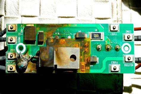
Burned or Charred PCB Traces
When excessive current flows through a PCB trace, it can generate heat and cause the trace to burn or char. This damage is often localized and can be identified by visual inspection.
Delamination of PCB Layers
PCBs are typically made of multiple layers of insulating material and conductive traces. If the bonding between these layers is compromised due to overheating or mechanical stress, delamination can occur. This can lead to poor electrical connections and reduced structural integrity of the PCB.
Component Damage
Current diversion and low resistance can also damage individual components on a PCB. This can include:
- Burned or overheated components
- Cracked or broken components
- Shorted or open components
Component damage can cause the PCB to malfunction or fail completely.

Preventing PCB Damage
To minimize the risk of PCB damage caused by current diversion and low resistance, several preventive measures can be taken:
Proper PCB Design
Designing a PCB with appropriate trace widths, spacing, and component placement can help prevent current diversion and ensure proper resistance. Additionally, incorporating protection features such as fuses and circuit breakers can help limit the impact of excessive current.
Quality Control and Testing
Thorough quality control and testing procedures during PCB manufacturing can help identify and address potential issues before the PCB is put into use. This can include:
- Visual inspection for defects and contaminants
- Electrical testing to ensure proper connectivity and resistance
- Environmental testing to evaluate the PCB’s resilience to temperature, humidity, and other factors
Proper Handling and Storage
PCBs should be handled and stored in a way that minimizes the risk of damage. This includes:
- Using ESD-safe handling procedures and equipment
- Storing PCBs in a clean, dry, and temperature-controlled environment
- Avoiding mechanical stress or impact during handling and transportation
Regular Maintenance and Inspection
Regularly inspecting and maintaining PCBs can help identify and address potential issues before they cause significant damage. This can include:
- Cleaning the PCB to remove contaminants and debris
- Checking for signs of overheating, discoloration, or deformation
- Testing electrical connections and components for proper functionality
By implementing these preventive measures, the risk of PCB damage caused by current diversion and low resistance can be significantly reduced.

Case Studies
To better understand the impact of current diversion and low resistance on PCBs, let’s examine a few real-world case studies.
Case Study 1: Smartphone Charger Failure
A smartphone manufacturer received numerous complaints about chargers failing after a short period of use. Upon investigation, it was discovered that a manufacturing defect in the PCB was causing current diversion, leading to overheating and component damage. The manufacturer had to recall the affected chargers and implement stricter quality control measures to prevent future issues.
Case Study 2: Industrial Control System Malfunction
An industrial facility experienced unexpected shutdowns and malfunctions in its control system. The problem was traced back to a PCB in the system that had developed low resistance due to exposure to high humidity levels. The PCB was replaced, and the facility implemented better environmental controls to prevent future occurrences.
Case Study 3: Automotive Electronics Failure
A car manufacturer received reports of various electronic systems failing in their vehicles. Investigation revealed that the PCBs used in these systems were susceptible to current diversion caused by vibration and mechanical stress. The manufacturer had to redesign the PCBs and improve their mounting to address the issue.
These case studies highlight the importance of proper PCB design, manufacturing, and maintenance in preventing damage caused by current diversion and low resistance.

Frequently Asked Questions (FAQ)
-
What are the signs of PCB damage caused by current diversion or low resistance?
Signs of PCB damage may include burned or charred traces, discoloration, deformation, or visible damage to components. The PCB may also malfunction or fail completely. -
Can PCB damage be repaired?
In some cases, minor PCB damage can be repaired by replacing damaged components or traces. However, more extensive damage may require the complete replacement of the PCB. -
How can I test a PCB for current diversion or low resistance?
PCBs can be tested using various methods, including visual inspection, continuity testing, and resistance measurement. Specialized equipment such as a multimeter or oscilloscope may be required for accurate testing. -
What should I do if I suspect my PCB has been damaged by current diversion or low resistance?
If you suspect PCB damage, it is important to stop using the affected device immediately to prevent further damage or potential safety hazards. Consult with a qualified technician or the manufacturer for guidance on repair or replacement options. -
How can I ensure the quality and reliability of PCBs in my products?
To ensure PCB quality and reliability, it is important to work with reputable PCB manufacturers that follow strict quality control and testing procedures. Additionally, proper PCB design, handling, and maintenance practices should be followed throughout the product lifecycle.
Conclusion
PCB damage caused by current diversion and low resistance is a serious issue that can lead to device malfunction, safety hazards, and financial losses. By understanding the causes and effects of this type of damage, and implementing proper prevention and maintenance strategies, the risk of PCB failure can be significantly reduced. As technology continues to advance, it is crucial for manufacturers, designers, and users to prioritize PCB quality and reliability to ensure the safe and effective operation of electronic devices.


Leave a Reply