Introduction to Rigid PCB Boards
A printed circuit board (PCB) is a board used to mechanically support and electrically connect electronic components using conductive tracks, pads and other features. Rigid PCBs are the most common type of PCBs and are made of rigid laminated sheets.
Rigid PCB boards provide a sturdy base for mounting and interconnecting electronic components. They allow electrical currents to pass between attached components such as resistors and integrated circuits. Rigid PCBs are found in most electronic devices including computers, mobile phones, TVs, ATMs etc.
Some key advantages of using rigid PCB boards are:
- Durability – Rigid boards can withstand physical stress better than flexible boards. The laminated construction provides mechanical strength.
- Heat resistance – The typically used FR-4 material has good thermal conductivity and can withstand high temperatures.
- Cost-effectiveness – Rigid PCBs can be mass produced efficiently making them cost effective.
- Layout flexibility – Rigid boards allow for complex circuit routing and layouts.
- Component mounting – Components can be securely soldered onto rigid PCBs. Surface mount and through hole mounting are supported.
In this comprehensive guide, we will cover everything you need to know about rigid PCB boards including their design, materials, fabrication, assembly and testing.
Rigid PCB Board Design
Rigid PCBs need to be carefully designed before fabrication. This involves schematic capture, PCB layout, routing and component placement. Electronic design automation (EDA) software is used for the design process.
Some key considerations in rigid PCB design:
Schematic Capture
This involves creating a circuit diagram showing the components and connections. Symbols are used to depict parts like resistors, capacitors, ICs etc. Schematic capture lays the foundation for PCB layout.
PCB Layout
The physical dimensions, shape, layer stackup and locations of traces, pads, vias and holes are decided. Component footprints are assigned. Layout follows electrical and physical design rules.
Trace Routing
Traces or tracks are laid to create electrical connections between pads and components as per the schematic. Autorouters can route simpler PCBs automatically. Complex designs require manual routing.
Component Placement
The components need to be carefully placed on the PCB considering factors like symmetry, spacing, connection lengths, heat dissipation etc. Effective component placement optimizes PCB performance.
Design Rule Checks
The completed layout needs to be verified against electrical and physical constraints like trace width, clearance, via sizes, mask margins, annular rings etc. Design rule checks (DRC) ensure proper manufacturability.
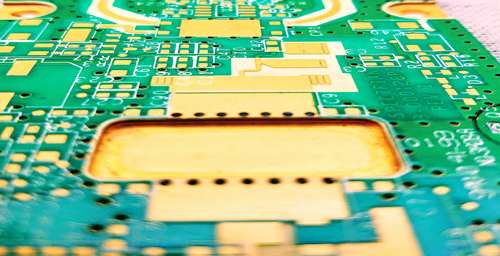
Rigid PCB Board Materials
Rigid PCB substrates are made using laminates that sandwich copper layers between insulating dielectric materials. The common rigid PCB materials include:
FR-4
FR-4 glass epoxy is the most popular and cost-effective rigid PCB material. It consists of woven fiberglass cloth with an epoxy resin binder that provides mechanical strength. FR-4 has good physical, electrical, thermal, chemical and moisture resistant properties.
CEM-1
Cellulose paper reinforced epoxy known as CEM-1 offers better electrical performance than FR-4. It has lower loss and stable dielectric constant over frequency. CEM-1 has excellent thermal conductivity but lower mechanical strength.
Polyimide
Polyimide laminates like Kapton offer very high temperature resistance. However polyimide is more expensive than FR-4. Rigid-flex PCBs often use polyimide flexible layers.
Rogers
Rogers corporation provides high frequency laminates like RO3003 and RO4003. These have stable dielectric constants across microwave and mm-wave frequencies. Rogers boards are more expensive but required for high frequency applications.
Aluminum
Aluminum PCBs use aluminum as the conductive layer instead of copper. They have excellent thermal conductivity to dissipate heat. But aluminum is not as conductive as copper.
Rigid PCB Board Fabrication
Rigid PCBs are fabricated using processes like imaging, etching, lamination, drilling, plating, routing and milling.
Lamination
Sheets of copper clad laminate are stacked up in a book-like manner based on the layer count. Prepreg bonding sheets are inserted in between. The stack is laminated under high pressure and temperature to form a solid PCB panel.
Imaging
A photosensitive dry film is applied on the copper layers. The PCB layout patterns are printed on the layers using exposure units. The unexposed dry film is then chemically washed away.
Etching
The exposed copper without photoresist is etched away chemically leaving only the desired copper traces. Common etching techniques are wet etching, dry etching and plasma etching.
Drilling
Holes are drilled at component mounting locations and for vias to interconnect layers. Mechanical, laser, plasma and abrasive jet drilling methods are used.
Plating
The walls of drilled holes are plated with copper to form a conductive barrel. Electroless copper followed by electrolytic copper plating is applied.
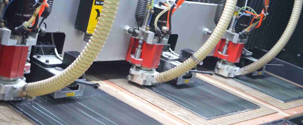
Routing and Milling
A spiral router separates individual PCBs from the panel. Edge profiling, cutouts, slots and grooves are created using milling machines.
Soldermask and Silkscreen
Soldermask is a protective insulation layer applied over the top and bottom copper layers. Silkscreen provides component designators, logos and other markings.
Surface Finish
An outer surface finish like ENIG, immersion tin or HASL is applied. This protects the exposed copper from oxidation.
Rigid PCB Board Assembly
After fabrication, electronic components need to be assembled and soldered onto the bare rigid PCBs. This is done using two main techniques:
Through Hole Assembly
Leaded components are inserted into holes in the PCB and soldered for both electrical and mechanical connection. Wave soldering machines are commonly used for TH assembly.
Surface Mount Assembly
SMD components are placed onto PCB pads using pick and place machines. Reflow soldering melts solder paste to attach components. SMT allows high density component loading.
In addition to soldering, adhesives are sometimes used to mount large electromechanical parts. Connectors need to be manually pressed into plated through holes.
Rigid PCB Board Testing
Rigid boards need to be tested to ensure there are no electrical shorts, opens or other faults. Common PCB testing methods include:
- ICT (In-Circuit Test): Tests components and connections while powered up. Checks for incorrectly assembled parts, wrong values, misalignments etc.
- Flying Probe Test: Uses movable probes to test connectivity between different test points on the board without fixtures.
- JTAG/Boundary Scan: Tests interconnects between components with Boundary Scan capability. Needs access to netlist.
- AOI (Automated Optical Inspection): Optically examines assembled PCBs for defects like missing parts, tombstoning, skewed parts etc.
- X-Ray Imaging: X-ray inspection can detect issues like shorts, open vias, voiding in solder joints etc.
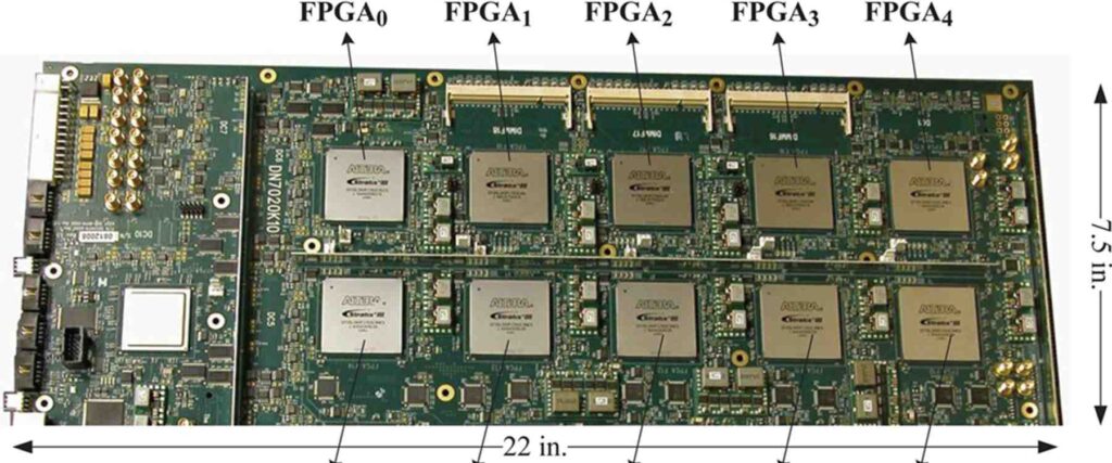
Applications of Rigid PCB Boards
Some common applications and products that use rigid PCB boards include:
- Computers – Motherboards, graphics cards, storage devices
- Consumer Electronics – Mobile phones, TVs, game consoles, wearables
- Automotive – Engine control units, infotainment systems, ADAS modules
- Medical Equipment – Imaging systems, analyzers, monitors
- Industrial – Programmable logic controllers, robotics systems
- Telecommunication – Routers, base stations, switches, transceivers
- Military/Aerospace – Avionics systems, radars, guidance systems
- Scientific – Lab instruments, test equipment, measurement devices
With the growth of electronics, use of rigid PCBs is increasing in almost every domain and will continue to remain a crucial component in electronic devices and systems.
FQA on Rigid PCB Boards
Here are some frequently asked questions about rigid PCB boards:
Q1. What are the typical layer counts for rigid PCB boards?
Rigid PCBs can have anywhere from 1 to 60 layers or more. Some common layer counts are:
- 2-4 layers – Common in cost-sensitive consumer electronics
- 6-10 layers – Used in networking/telecom, automotive, industrial electronics
- 12+ layers – Found in high density interconnection boards, servers etc.
Q2. What are some important design rules to follow for rigid PCBs?
Some key rigid PCB design rules involve:
- Trace width based on current and PCB thickness
- Trace clearance between conductors
- Via padsizes and anti-pad clearances
- Minimum hole sizes for vias and component leads
- Soldermask expansion from pads
- Keepout areas around drill holes
Q3. What are the limitations of rigid PCB boards?
Some limitations of rigid PCBs are:
- Lack of flexibility makes them unsuitable for dynamic flexing environments
- Limited thermal conductivity for very high power devices
- Difficult to repair or modify once fabricated
- Max PCB size limited by fabrication equipment
- Prone to cracking and breaking under physical or thermal stress
Q4. How are rigid and flexible PCBs different?
Key differences between rigid and flexible PCBs:
- Rigid PCBs use stiff insulating substrates while flex PCBs use flexible dielectric films.
- Rigid PCBs offer better mechanical strength while flex PCBs can withstand repeated bending.
- Rigid PCBs have higher layer counts and component densities vs flex PCBs.
- Rigid PCBs are more suited for complex high-density layouts vs simple flex circuits.
- Rigid PCBs are cheaper in medium to high volumes while flex PCBs cost less in prototypes.
Q5. What are some advanced rigid PCB technologies?
Some advanced rigid PCB fabrication technologies are:
- HDI (High Density Interconnect) to enable high trace densities
- Any-layer HDI allowing traces between any layers
- Buried and blind vias to optimize routing
- Microvias (below 0.15mm) for dense interconnects
- Embedded passives for increased functionality
- Heavy copper up to 400g/m2 to handle high currents
- Impedance controlled traces for high speed signals
So in summary, rigid PCB technology continues to evolve enabling greater miniaturization, component densities, operating frequencies, power levels and functionality.


Leave a Reply